SBVS271A October   2015  – February 2024 TPS3710

PRODUCTION DATA  

  1.   1
  2. Features
  3. Applications
  4. Description
  5. Pin Configuration and Functions
  6. Specifications
    1. 5.1 Absolute Maximum Ratings
    2. 5.2 ESD Ratings
    3. 5.3 Recommended Operating Conditions
    4. 5.4 Thermal Information
    5. 5.5 Electrical Characteristics
    6. 5.6 Timing Requirements
    7. 5.7 Switching Characteristics
    8. 5.8 Typical Characteristics
  7. Detailed Description
    1. 6.1 Overview
    2. 6.2 Functional Block Diagram
    3. 6.3 Feature Description
      1. 6.3.1 Input (SENSE)
      2. 6.3.2 Output (OUT)
      3. 6.3.3 Immunity to Input-Pin Voltage Transients
    4. 6.4 Device Functional Modes
      1. 6.4.1 Normal Operation (VDD > UVLO)
      2. 6.4.2 Undervoltage Lockout (V(POR) < VDD < UVLO)
      3. 6.4.3 Power-On Reset (VDD < V(POR))
  8. Application and Implementation
    1. 7.1 Application Information
      1. 7.1.1 VPULLUP to a Voltage Other Than VDD
      2. 7.1.2 Monitoring VDD
      3. 7.1.3 Monitoring a Voltage Other Than VDD
    2. 7.2 Typical Application
      1. 7.2.1 Design Requirements
      2. 7.2.2 Detailed Design Procedure
        1. 7.2.2.1 Resistor Divider Selection
        2. 7.2.2.2 Pullup Resistor Selection
        3. 7.2.2.3 Input Supply Capacitor
        4. 7.2.2.4 Sense Capacitor
      3. 7.2.3 Application Curve
    3. 7.3 Do's and Don'ts
    4. 7.4 Power-Supply Recommendations
    5. 7.5 Layout
      1. 7.5.1 Layout Guidelines
      2. 7.5.2 Layout Example
  9. Device and Documentation Support
    1. 8.1 Device Support
      1. 8.1.1 Device Nomenclature
    2. 8.2 Documentation Support
      1. 8.2.1 Related Documentation
    3. 8.3 Receiving Notification of Documentation Updates
    4. 8.4 Support Resources
    5. 8.5 Trademarks
    6. 8.6 Electrostatic Discharge Caution
    7. 8.7 Glossary
  10. Revision History
  11. 10Mechanical, Packaging, and Orderable Information

Package Options

Mechanical Data (Package|Pins)
Thermal pad, mechanical data (Package|Pins)
Orderable Information

Description

The TPS3710 wide supply voltage detector operates over a 1.8V to 18V range. The device has a high-accuracy comparator with an internal 400mV reference and an open-drain output rated to 18V for precision voltage detection. The monitored voltage can be set with the use of external resistors.

The OUT pin is driven low when the voltage at the SENSE pin drops below (VIT–), and goes high when the voltage returns above the respective threshold (VIT+). The comparator in the TPS3710 includes built-in hysteresis for filtering to reject brief glitches, which helps the device to operate without false triggering.

The TPS3710 is available in a 6-pin SOT package, and a 1.5mm × 1.5mm 6-pin WSON package, and is specified over the junction temperature range of –40°C to +125°C.

Device Information
PART NUMBERPACKAGE(1)BODY SIZE (NOM) (2)
TPS3710SOT (6)2.90mm × 1.60mm
WSON (6)1.50mm × 1.50mm
For all available packages, see the package option addendum at the end of the data sheet.
The package size (length × width) is a nominal value and includes pins, where applicable.
GUID-A4822366-2EDA-4D71-BE97-B5D1BD00AB5E-low.svgSimplified Schematic
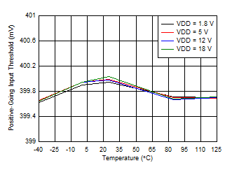
GUID-64A080E9-0AF4-4ABC-B1B1-585D8AF01F1D-low.gifRising Input Threshold Voltage (VIT+) vs Temperature