SBVS085J January   2007  – June 2017

PRODUCTION DATA.  

  1. Features
  2. Applications
  3. Description
  4. Revision History
  5. Device Comparison Table
  6. Pin Configuration and Functions
  7. Specifications
    1. 7.1 Absolute Maximum Ratings
    2. 7.2 ESD Ratings
    3. 7.3 Recommended Operating Conditions
    4. 7.4 Thermal Information
    5. 7.5 Electrical Characteristics
    6. 7.6 Timing Requirements
    7. 7.7 Typical Characteristics
  8. Detailed Description
    1. 8.1 Overview
    2. 8.2 Functional Block Diagrams
    3. 8.3 Feature Description
      1. 8.3.1 Immunity to SENSE Pin Voltage Transients
      2. 8.3.2 SENSE Input
      3. 8.3.3 Manual Reset (MR) Input
      4. 8.3.4 Selecting the Reset Delay Time
    4. 8.4 Device Functional Modes
  9. Applications and Implementation
    1. 9.1 Application Information
    2. 9.2 Typical Application
      1. 9.2.1 Design Requirements
      2. 9.2.2 Detailed Design Procedure
      3. 9.2.3 Application Curves
  10. 10Power Supply Recommendations
  11. 11Layout
    1. 11.1 Layout Guidelines
    2. 11.2 Layout Example
  12. 12Device and Documentation Support
    1. 12.1 Related Links
    2. 12.2 Receiving Notification of Documentation Updates
    3. 12.3 Community Resources
    4. 12.4 Trademarks
    5. 12.5 Electrostatic Discharge Caution
    6. 12.6 Glossary
  13. 13Mechanical, Packaging, and Orderable Information

Package Options

Mechanical Data (Package|Pins)
Thermal pad, mechanical data (Package|Pins)
Orderable Information

Layout

Layout Guidelines

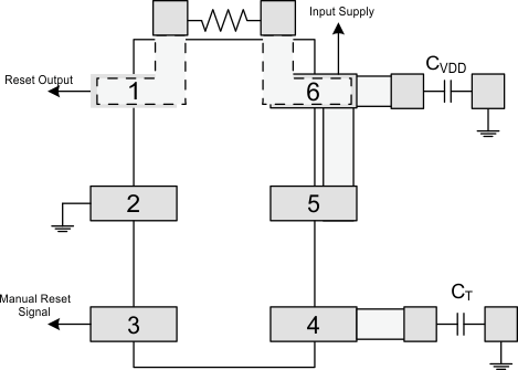
TI recommends placing the 0.1-µF decoupling capacitor close to the VDD pin. The VDD trace should be able to carry 6 µA without a significant drop in voltage.

Layout Example

TPS3808G01-Q1 TPS3808G12-Q1 TPS3808G125-Q1 TPS3808G15-Q1 TPS3808G18-Q1 TPS3808G30-Q1 TPS3808G33-Q1 TPS3808G50-Q1 Layout_Example_sbvs085.gif Figure 18. Recommended Layout