SGLS142C December 2002 – December 2020
PRODUCTION DATA
- 1 Features
- 2 Applications
- 3 Description
- 4 Revision History
- 5 Device Comparison
- 6 Pin Configuration and Functions
- 7 Specifications
- 8 Detailed Description
- 9 Application and Implementation
- 10Power Supply Recommendations
- 11Layout
- 12Device and Documentation Support
- 13Mechanical, Packaging, and Orderable Information
Package Options
Refer to the PDF data sheet for device specific package drawings
Mechanical Data (Package|Pins)
- DBV|3
Thermal pad, mechanical data (Package|Pins)
Orderable Information
3 Description
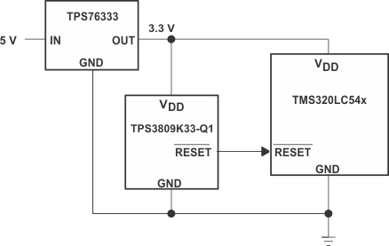
The TPS3809 family of supervisory circuits provides circuit initialization and timing supervision, primarily for DSPs and processor-based systems. The newer TLV809E device is an alternative with the same pins, functions and electrical parameters.
During power-on, RESET is asserted when the supply voltage VDD becomes higher than 1.1 V. Thereafter, the supervisory circuit monitors VDD and keeps RESET active as long as VDD remains below the threshold voltage VIT. An internal timer delays the return of the output to the inactive state (high) to ensure proper system reset. The delay time, td(typ) = 200 ms, starts after VDD has risen above the threshold voltage VIT. When the supply voltage drops below the threshold voltage VIT, the output becomes active (low) again. No external components are required. All the devices of this family have a fixed sense-threshold voltage VIT set by an internal voltage divider.
The product spectrum is designed for supply voltages of 2.5 V, 3 V, 3.3 V, and 5 V. The circuits are available in a 3-pin SOT-23. The TPS3809xxx-Q1 devices are characterized for operation over a temperature range of −40°C to 125°C, and are qualified in accordance with AEC-Q100 stress test qualification for integrated circuits.
| PART NUMBER | PACKAGE | BODY SIZE (NOM) |
|---|---|---|
| TPS3809xxx-Q1 | SOT-23 (3) | 2.90 mm × 1.60 mm |
 Typical Application