SBVS285 February   2017 TPS3852-Q1

PRODUCTION DATA.  

  1. Features
  2. Applications
  3. Description
    1.     Device Images
      1.      Typical Application Circuit
      2.      Undervoltage Threshold (VITN) Accuracy vs Temperature
  4. Revision History
  5. Pin Configuration and Functions
    1.     Pin Functions
  6. Specifications
    1. 6.1 Absolute Maximum Ratings
    2. 6.2 ESD Ratings
    3. 6.3 Recommended Operating Conditions
    4. 6.4 Thermal Information
    5. 6.5 Electrical Characteristics
    6. 6.6 Timing Requirements
    7. 6.7 Typical Characteristics
  7. Detailed Description
    1. 7.1 Overview
    2. 7.2 Functional Block Diagram
    3. 7.3 Feature Description
      1. 7.3.1 RESET
      2. 7.3.2 Manual Reset (MR)
      3. 7.3.3 Undervoltage Fault Detection
      4. 7.3.4 Watchdog Mode
        1. 7.3.4.1 SET1
        2. 7.3.4.2 Window Watchdog Timer
        3. 7.3.4.3 Watchdog Input (WDI)
        4. 7.3.4.4 CWD
        5. 7.3.4.5 Watchdog Output (WDO)
    4. 7.4 Device Functional Modes
      1. 7.4.1 VDD is Below VPOR (VDD < VPOR)
      2. 7.4.2 Above Power-On-Reset, But Less Than VDD(min) (VPOR ≤ VDD < VDD(min))
      3. 7.4.3 Normal Operation (VDD ≥ VDD(min))
  8. Application and Implementation
    1. 8.1 Application Information
      1. 8.1.1 CWD Functionality
        1. 8.1.1.1 Factory-Programmed Timing Options
        2. 8.1.1.2 Adjustable Capacitor Timing
      2. 8.1.2 Overdrive Voltage
    2. 8.2 Typical Application
      1. 8.2.1 Design Requirements
      2. 8.2.2 Detailed Design Procedure
        1. 8.2.2.1 Monitoring the 3.3-V Rail
        2. 8.2.2.2 Calculating RESET and the WDO Pullup Resistor
        3. 8.2.2.3 Setting the Window Watchdog
        4. 8.2.2.4 Watchdog Disabled During Initialization Period
      3. 8.2.3 Glitch Immunity
      4. 8.2.4 Application Curves
  9. Power Supply Recommendations
  10. 10Layout
    1. 10.1 Layout Guidelines
    2. 10.2 Layout Example
  11. 11Device and Documentation Support
    1. 11.1 Device Support
      1. 11.1.1 Development Support
        1. 11.1.1.1 Evaluation Module
      2. 11.1.2 Device Nomenclature
    2. 11.2 Receiving Notification of Documentation Updates
    3. 11.3 Community Resources
    4. 11.4 Trademarks
    5. 11.5 Electrostatic Discharge Caution
    6. 11.6 Glossary
  12. 12Mechanical, Packaging, and Orderable Information

Package Options

Refer to the PDF data sheet for device specific package drawings

Mechanical Data (Package|Pins)
  • DRB|8
Thermal pad, mechanical data (Package|Pins)
Orderable Information

Overdrive Voltage

Forcing a RESET is dependent on two conditions: the amplitude VDD is beyond the trip point (ΔV1 and ΔV2), and the length of time that the voltage is beyond the trip point (t1 and t2). If the voltage is just under the trip point for a long period of time, RESET asserts and the output is pulled low. However, if VDD is just under the trip point for a few nanoseconds, RESET does not assert and the output remains high. The length of time required for RESET to assert can be changed by increasing the amount VDD goes under the trip point. If VDD is under the trip point by 10%, the amount of time required for the comparator to respond is much faster and causes RESET to assert much quicker than when barely under the trip point voltage. Equation 2 shows how to calculate the percentage overdrive.

Equation 2. Overdrive = |( VDD / VITX – 1) × 100% |

In Equation 2, VITX corresponds to the threshold trip point. If VDD is exceeding the positive threshold, VITN + VHYST is used. VITN is used when VDD is falling below the negative threshold. In Figure 19, t1 and t2 correspond to the amount of time that VDD is over the threshold; the propagation delay versus overdrive for VITN and VITN + VHYST is illustrated in Figure 13 and Figure 14, respectively.

The TPS3852-Q1 is relatively immune to short positive and negative transients on VDD because of the overdrive voltage.
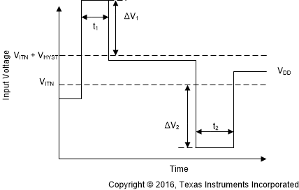
TPS3852-Q1 Overdrive_sbvs302.gifFigure 19. Overdrive Voltage