SBVS105F September   2009  – October 2018 TPS386000 , TPS386040

PRODUCTION DATA.  

  1. Features
  2. Applications
  3. Description
    1.     Device Images
      1.      TPS386000 Typical Application Circuit: Monitoring Supplies for an FPGA
  4. Revision History
  5. Pin Configuration and Functions
    1.     Pin Functions
  6. Specifications
    1. 6.1 Absolute Maximum Ratings
    2. 6.2 ESD Ratings
    3. 6.3 Recommended Operating Conditions
    4. 6.4 Thermal Information
    5. 6.5 Electrical Characteristics
    6. 6.6 Timing Requirements
    7. 6.7 Switching Characteristics
    8. 6.8 Typical Characteristics
  7. Parameter Measurement Information
  8. Detailed Description
    1. 8.1 Overview
    2. 8.2 Functional Block Diagrams
    3. 8.3 Feature Description
      1. 8.3.1 Voltage Monitoring
      2. 8.3.2 Manual Reset
      3. 8.3.3 Watchdog Timer
      4. 8.3.4 Reset Output
    4. 8.4 Device Functional Modes
  9. Application and Implementation
    1. 9.1 Application Information
      1. 9.1.1 Undervoltage Detection
      2. 9.1.2 Undervoltage and Overvoltage Detection
      3. 9.1.3 Sensing a Negative Voltage
      4. 9.1.4 Reset Delay Time
    2. 9.2 Typical Application
      1. 9.2.1 Design Requirements
      2. 9.2.2 Detailed Design Procedure
      3. 9.2.3 Application Curves
  10. 10Power Supply Recommendations
  11. 11Layout
    1. 11.1 Layout Guidelines
    2. 11.2 Layout Example
  12. 12Device and Documentation Support
    1. 12.1 Device Support
      1. 12.1.1 Development Support
        1. 12.1.1.1 Evaluation Modules
        2. 12.1.1.2 Spice Models
      2. 12.1.2 Device Nomenclature
    2. 12.2 Documentation Support
      1. 12.2.1 Related Documentation
    3. 12.3 Related Links
    4. 12.4 Community Resources
    5. 12.5 Trademarks
    6. 12.6 Electrostatic Discharge Caution
    7. 12.7 Glossary
  13. 13Mechanical, Packaging, and Orderable Information

Package Options

Mechanical Data (Package|Pins)
Thermal pad, mechanical data (Package|Pins)
Orderable Information

Typical Characteristics

At TA = 25°C, and VDD = 3.3 V, with both options (TPS386000 and TPS386040) having the same characteristics, unless otherwise noted.
TPS386000 TPS386040 tc_icc-vcc_bvs105.gif
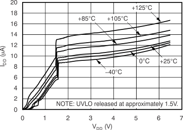
Figure 8. TPS386040 Supply Current vs Supply Voltage
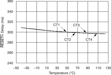
TPS386000 TPS386040 tc_reset-tmp_open_bvs105.gif
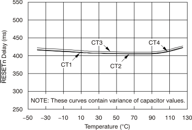
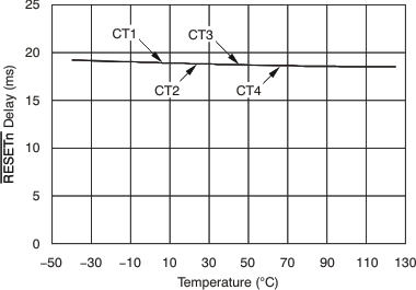
Figure 10. TPS386040 (CTn = Open) RESETn Time-out Period vs Temperature
TPS386000 TPS386040 tc_reset-tmp_01uf_bvs105.gif
Figure 12. TPS386040 (CTn = 0.1 µF) RESETn Time-out Period vs Temperature
TPS386000 TPS386040 tc_sense-overdrive_bvs105.gif
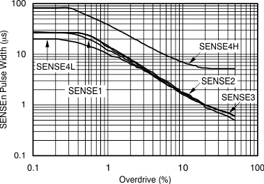
See Figure 29 for measurement technique
Figure 14. TPS386040 SENSEn Minimum Pulse Width
vs SENSEn Threshold Overdrive Voltage
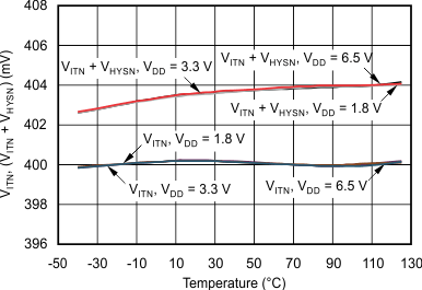
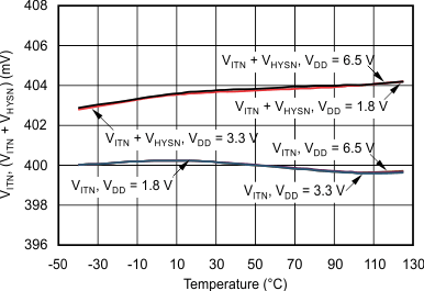
TPS386000 TPS386040 tc_sense2-tmp_bvs105.gif
Figure 16. TPS386040 SENSE2 Threshold Voltage vs Temperature
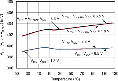
TPS386000 TPS386040 tc_sense4l-tmp_bvs105.gif
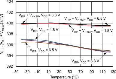
Figure 18. TPS386040 SENSE4L Threshold Voltage vs Temperature
TPS386000 TPS386040 tc_vout_low-iout_bvs105.gif
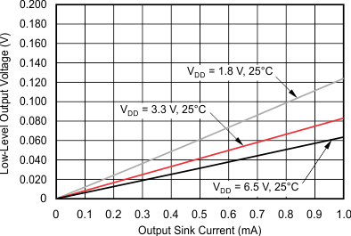
Figure 20. Output Voltage Low vs Output Current
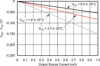
TPS386000 TPS386040 tc_vout_high-iout_bvs105.gif
Figure 22. Output Voltage High vs Output Current
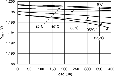
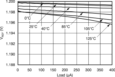
TPS386000 TPS386040 tc_vref-load_18v_bvs105.gif
Figure 24. TPS386040 VREF Output Load Regulation
(VDD = 1.8 V)
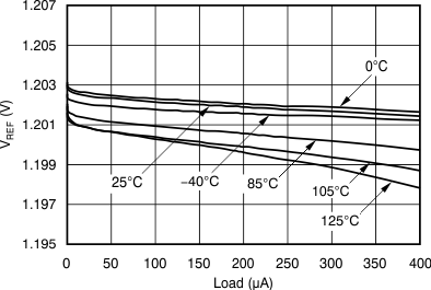
TPS386000 TPS386040 tc_vref-load_65v_bvs105.gif
Figure 26. TPS386040 VREF Output Load Regulation
(VDD = 6.5 V)
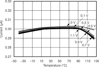
TPS386000 TPS386040 tc_pin_charge-tmp_bvs105.gif
Figure 28. TPS386040 CT1 to CT4 Pin Charging Current vs Temperature Over CT Pin Voltage
TPS386000 TPS386040 tc_reset-ct_bvs105.gif
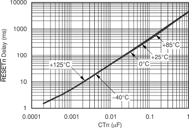
Figure 9. TPS386040 RESETn Time-out Period vs CTn
TPS386000 TPS386040 tc_reset-tmp_vcc_bvs105.gif
Figure 11. TPS386040 (CTn = VDD) RESETn Time-out Period vs Temperature
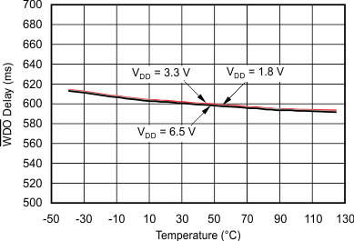
TPS386000 TPS386040 tc_wdo-tmp_bvs105.gif
Figure 13. TPS386040 WDO Time-out Period vs Temperature
TPS386000 TPS386040 tc_sense1-tmp_bvs105.gif
Figure 15. TPS386040 SENSE1 Threshold Voltage vs Temperature
TPS386000 TPS386040 tc_sense3-tmp_bvs105.gif
Figure 17. TPS386040 SENSE3 Threshold Voltage vs Temperature
TPS386000 TPS386040 tc_sense4h-tmp_bvs105.gif
Figure 19. TPS386040 SENSE4H Threshold Voltage vs Temperature
TPS386000 TPS386040 tc_vout_low-tmp_bvs105.gif
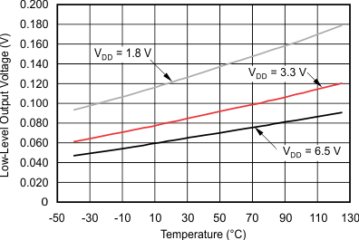
Figure 21. Output Voltage Low at 1 mA vs Temperature
TPS386000 TPS386040 tc_vout_high-tmp_bvs105.gif
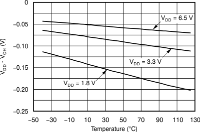
Figure 23. Output Voltage High at 1 mA vs Temperature
TPS386000 TPS386040 tc_vref-load_33v_bvs105.gif
Figure 25. TPS386040 VREF Output Load Regulation
(VDD = 3.3 V)
TPS386000 TPS386040 tc_vref-tmp_bvs105.gif
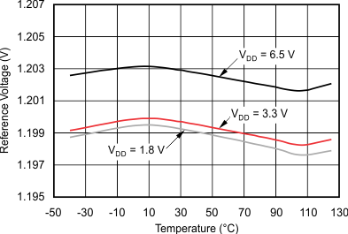
Figure 27. TPS386040 VREF at 0 µA vs Temperature