SLUS593J December 2003 – June 2022 TPS40054 , TPS40055 , TPS40057
PRODUCTION DATA
- 1 Features
- 2 Applications
- 3 Description
- 4 Revision History
- 5 Pin Configuration and Functions
- 6 Specifications
-
7 Detailed Description
- 7.1 Overview
- 7.2 Functional Block Diagram
- 7.3
Feature Description
- 7.3.1 Setting the Switching Frequency (Programming the Clock Oscillator)
- 7.3.2 Programming The Ramp Generator Circuit
- 7.3.3 UVLO Operation
- 7.3.4 BP5 and BP10 Internal Voltage Regulators
- 7.3.5 Programming Soft Start
- 7.3.6 Programming Current Limit
- 7.3.7 Synchronizing to an External Supply
- 7.3.8 Loop Compensation
- 7.4 Device Functional Modes
-
8 Application and Implementation
- 8.1 Application Information
- 8.2
Typical Application
- 8.2.1 Design Requirements
- 8.2.2
Detailed Design Procedure
- 8.2.2.1 Calculate Maximum and Minimum Duty Cycles
- 8.2.2.2 Select Switching Frequency
- 8.2.2.3 Select ΔI
- 8.2.2.4 Calculate the High-Side MOSFET Power Losses
- 8.2.2.5 Calculate Synchronous Rectifier Losses
- 8.2.2.6 Calculate the Inductor Value
- 8.2.2.7 Set the Switching Frequency
- 8.2.2.8 Program the Ramp Generator Circuit
- 8.2.2.9 Calculate the Output Capacitance (CO)
- 8.2.2.10 Calculate the Soft-Start Capacitor (CSS/SD)
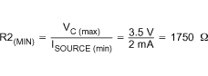
- 8.2.2.11 Calculate the Current Limit Resistor (RILIM)
- 8.2.2.12 Calculate Loop Compensation Values
- 8.2.2.13 Calculate the Boost and BP10V Bypass Capacitance
- 8.2.3 Application Curves
- 9 Power Supply Recommendations
- 10Layout
- 11Device and Documentation Support
- 12Mechanical, Packaging, and Orderable Information
Package Options
Refer to the PDF data sheet for device specific package drawings
Mechanical Data (Package|Pins)
- PWP|16
Thermal pad, mechanical data (Package|Pins)
- PWP|16
Orderable Information
7.3.8 Loop Compensation
Voltage-mode buck-type converters are typically compensated using Type III networks. Since the TPS4005x uses voltage feedforward control, the gain of the PWM modulator with voltage feedforward circuit must be included. The generic modulator gain is described in Figure 7-5. Duty cycle, D, varies from 0 to 1 as the control voltage, VC, varies from the minimum ramp voltage to the maximum ramp voltage, VS. Also, for a synchronous buck converter, D = VO / VIN. To get the control voltage to output voltage modulator gain in terms of the input voltage and ramp voltage:
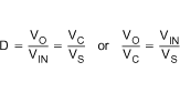
With the voltage feedforward function, the ramp slope is proportional to the input voltage. Therefore, the moderator DC gain is independent to the change of input voltage.
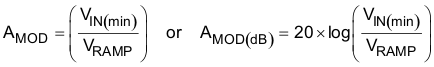
For the TPS4005x, with VIN(min) being the minimum input voltage required to cause the ramp excursion to reach the maximum ramp amplitude of VRAMP, the modulator DC gain is shown in Equation 12.
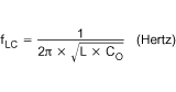
For a buck converter using voltage mode control, there is a double pole due to the output L-CO. The double pole is located at the frequency calculated in Equation 13.
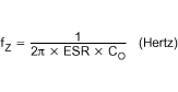
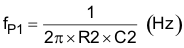
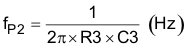
There is also a zero created by the output capacitance, CO, and its associated ESR. The ESR zero is located at the frequency calculated in Equation 14.
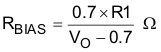
Calculate the value of RBIAS to set the output voltage, VO.
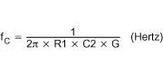
The maximum crossover frequency (0 dB loop gain) is set by Equation 16.

Typically, fC is selected to be close to the midpoint between the L-CO double pole and the ESR zero. At this frequency, the control to output gain has a –2 slope (–40 dB/decade), while the Type III topology has a +1 slope (20 dB/decade), resulting in an overall closed loop –1 slope (–20 dB/decade). Figure 7-6 shows the modulator gain, L-C filter, output capacitor ESR zero, and the resulting response to be compensated.


A Type III topology, shown in Figure 7-7, has two zero-pole pairs in addition to a pole at the origin. The gain and phase boost of a Type III topology is shown in Figure 7-8. The two zeros are used to compensate the L-CO double pole and provide phase boost. The double pole is used to compensate for the ESR zero and provide controlled gain roll-off. In many cases, the second pole can be eliminated and the gain roll-off of the amplifier is used to roll-off the overall gain at higher frequencies.


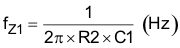
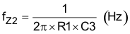
The poles and zeros for a Type III network are described in Equation 17 through Equation 20.
The value of R1 is somewhat arbitrary, but influences other component values. A value between 50 kΩ and 100 kΩ usually yields reasonable values.
The unity gain frequency is described in Equation 21.
where
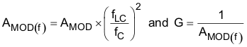
- G is the reciprocal of the modulator gain at fC.
The modulator gain as a function of frequency at fC is described in Equation 22.
Care must be taken not to load down the output of the error amplifier with the feedback resistor, R2, that is too small. The error amplifier has a finite output source and sink current, which must be considered when sizing R2. A value that is too small does not allow the output to swing over its full range.