SLUS593J December 2003 – June 2022 TPS40054 , TPS40055 , TPS40057
PRODUCTION DATA
- 1 Features
- 2 Applications
- 3 Description
- 4 Revision History
- 5 Pin Configuration and Functions
- 6 Specifications
-
7 Detailed Description
- 7.1 Overview
- 7.2 Functional Block Diagram
- 7.3
Feature Description
- 7.3.1 Setting the Switching Frequency (Programming the Clock Oscillator)
- 7.3.2 Programming The Ramp Generator Circuit
- 7.3.3 UVLO Operation
- 7.3.4 BP5 and BP10 Internal Voltage Regulators
- 7.3.5 Programming Soft Start
- 7.3.6 Programming Current Limit
- 7.3.7 Synchronizing to an External Supply
- 7.3.8 Loop Compensation
- 7.4 Device Functional Modes
-
8 Application and Implementation
- 8.1 Application Information
- 8.2
Typical Application
- 8.2.1 Design Requirements
- 8.2.2
Detailed Design Procedure
- 8.2.2.1 Calculate Maximum and Minimum Duty Cycles
- 8.2.2.2 Select Switching Frequency
- 8.2.2.3 Select ΔI
- 8.2.2.4 Calculate the High-Side MOSFET Power Losses
- 8.2.2.5 Calculate Synchronous Rectifier Losses
- 8.2.2.6 Calculate the Inductor Value
- 8.2.2.7 Set the Switching Frequency
- 8.2.2.8 Program the Ramp Generator Circuit
- 8.2.2.9 Calculate the Output Capacitance (CO)
- 8.2.2.10 Calculate the Soft-Start Capacitor (CSS/SD)
- 8.2.2.11 Calculate the Current Limit Resistor (RILIM)
- 8.2.2.12 Calculate Loop Compensation Values
- 8.2.2.13 Calculate the Boost and BP10V Bypass Capacitance
- 8.2.3 Application Curves
- 9 Power Supply Recommendations
- 10Layout
- 11Device and Documentation Support
- 12Mechanical, Packaging, and Orderable Information
Package Options
Refer to the PDF data sheet for device specific package drawings
Mechanical Data (Package|Pins)
- PWP|16
Thermal pad, mechanical data (Package|Pins)
- PWP|16
Orderable Information
7.3.3 UVLO Operation
The TPS4005x uses variable (user-programmable) UVLO protection. See the Programming the Ramp Generator section for more information on setting the UVLO voltage. The UVLO circuit holds the soft start low until the input voltage exceeds the user-programmable undervoltage threshold.
The TPS4005x uses the feedforward pin, KFF, as a user-programmable low-line UVLO detection. This variable low-line UVLO threshold compares the PWM ramp duration to the oscillator clock period. An undervoltage condition exists if the TPS4005x receives a clock pulse before the ramp has reached 90% of its full amplitude. The ramp duration is a function of the ramp slope, which is directly related to the current into the KFF pin. The KFF current is a function of the input voltage and the resistance from KFF to the input voltage. The KFF resistor can be referenced to the oscillator frequency as described in Equation 2.
The programmable UVLO function uses a 3-bit counter to prevent spurious shutdowns or turn-ons due to spikes or fast line transients. When the counter reaches a total of seven counts in which the ramp duration is shorter than the clock cycle, a power-good signal is asserted and a soft start initiated, and the upper and lower MOSFETS are turned off.
Once the soft start is initiated, the UVLO circuit must see a total count of seven cycles in which the ramp duration is longer than the clock cycle before an undervoltage condition is declared (see Figure 7-2).
 Figure 7-2 Undervoltage Lockout Operation
The tolerance on the UVLO set point also affects the maximum duty cycle achievable. If the UVLO starts the device at 10% below the nominal start-up voltage, the maximum duty cycle is reduced approximately 10% at the nominal start-up voltage.
The impedance of the input voltage can cause the input voltage, at the controller, to sag when the converter starts to operate and draw current from the input source. Therefore, there is voltage hysteresis that prevents nuisance shutdowns at the UVLO point. With RT chosen to select the operating frequency and RKFF chosen to select the start-up voltage, the approximate amount of hysteresis voltage is shown in Figure 6-3.
Some applications can require an additional circuit to prevent false restarts at the UVLO voltage level. This applies to applications that have high impedance on the input voltage line or that have excessive ringing on the VIN line. The input voltage impedance can cause the input voltage to sag enough at start-up to cause a UVLO shutdown and subsequent restart. Excessive ringing can also affect the voltage seen by the device and cause a UVLO shutdown and restart. A simple external circuit provides a selectable amount of hysteresis to prevent the nuisance UVLO shutdown.
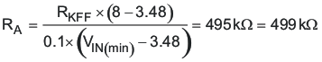
Assuming a hysteresis current of 10% IKFF, and the peak detector charges to 8 V and VIN(min) = 10 V, the value of RA is calculated by Equation 3 using a RKFF = 71.5 kΩ.
CA is chosen to maintain the peak voltage between switching cycles to keep the capacitor charge from drooping 0.1 V (from 8 V to 7.9 V).
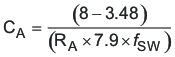
The value of CA can calculate to less than 10 pF, but some standard value up to 47 pF works adequately. The diode can be a small-signal switching diode or Schottky rated for more then 20 V. Figure 7-3 shows a typical implementation using a small switching diode.
The tolerance on the UVLO set point also affects the maximum duty cycle achievable. If the UVLO starts the device at 10% below the nominal start-up voltage, the maximum duty cycle is reduced approximately 10% at the nominal start-up voltage.
 Figure 7-3 Hysteresis for Programmable UVLO