SLUSD62 December 2017 TPS40345
PRODUCTION DATA.
- 1 Features
- 2 Applications
- 3 Description
- 4 Revision History
- 5 Pin Configuration and Functions
- 6 Specifications
- 7 Detailed Description
-
8 Application and Implementation
- 8.1 Application Information
- 8.2
Typical Applications
- 8.2.1 Design Requirements
- 8.2.2
Detailed Design Procedure
- 8.2.2.1 Selecting the Switching Frequency
- 8.2.2.2 Inductor Selection (L1)
- 8.2.2.3 Output Capacitor Selection (C12)
- 8.2.2.4 Peak Current Rating of Inductor
- 8.2.2.5 Input Capacitor Selection (C8)
- 8.2.2.6 MOSFET Switch Selection (Q1 and Q2)
- 8.2.2.7 Bootstrap Capacitor (C6)
- 8.2.2.8 VDD Bypass Capacitor (C7)
- 8.2.2.9 BP Bypass Capacitor (C5)
- 8.2.2.10 Short-Circuit Protection (R11)
- 8.2.2.11 Feedback Divider (R4, R5)
- 8.2.2.12 Compensation: (C2, C3, C4, R3, R6)
- 8.2.3 Application Curves
- 9 Power Supply Recommendations
- 10Layout
- 11Device and Documentation Support
- 12Mechanical, Packaging, and Orderable Information
Package Options
Mechanical Data (Package|Pins)
- DRC|10
Thermal pad, mechanical data (Package|Pins)
- DRC|10
Orderable Information
5 Pin Configuration and Functions
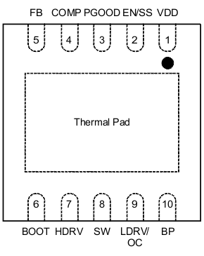
DRC Package
10-Pin VSON
Top View

Pin Functions
| PIN | I/O | DESCRIPTION | |
|---|---|---|---|
| NAME | NO. | ||
| BOOT | 6 | I | Gate drive voltage for the high-side N-channel MOSFET. A 0.1-µF capacitor (typical) must be connected between this pin and SW. For low input voltage operation, an external Schottky diode from BP to BOOT is recommended to maximize the gate drive voltage for the high-side. |
| BP | 10 | O | Output bypass for the internal regulator. Connect a low ESR bypass ceramic capacitor of 1 µF or greater from this pin to GND. |
| COMP | 4 | O | Output of the error amplifier and connection node for loop feedback components. |
| EN/SS | 2 | I | Logic level input which starts or stops the controller via an external user command. Letting this pin float turns the controller on. Pulling this pin low disables the controller. This is also the soft-start programming pin. A capacitor connected from this pin to GND programs the soft-start time. The capacitor is charged with an internal current source of 10 µA. The resulting voltage ramp of this pin is also used as a second non-inverting input to the error amplifier after a 0.8 V (typical) level shift downwards. Output regulation is controlled by the internal level shifted voltage ramp until that voltage reaches the internal reference voltage of 600 mV – the voltage ramp of this pin reaches 1.4 V (typical). Optionally, a 267-kΩ resistor from this pin to BP enables the FSS feature. |
| FB | 5 | I | Inverting input to the error amplifier. In normal operation, the voltage on this pin is equal to the internal reference voltage. |
| PGOOD | 3 | O | Open-drain power good output. |
| HDRV | 7 | O | Bootstrapped gate drive output for the high-side N-channel MOSFET. |
| LDRV/OC | 9 | O | Gate drive output for the low-side synchronous rectifier N-channel MOSFET. A resistor from this pin to GND is also used to determine the voltage level for OCP. An internal current source of 10 µA flows through the resistor during initial calibration and that sets up the voltage trip point used for OCP. |
| VDD | 1 | I | Power input to the controller. Bypass VDD to GND with a low ESR ceramic capacitor of at least 1 µF close to the device. |
| SW | 8 | O | Sense line for the adaptive anti-cross conduction circuitry. Serves as common connection for the flying high-side FET driver. |
| GND | Thermal Pad | — | Ground connection to the controller. This is also the thermal pad used to conduct heat from the device. This connection serves a twofold purpose. The first is to provide an electrical ground connection for the device. The second is to provide a low thermal impedance path from the device die to the PCB. This pad should be tied externally to a ground plane. |