SLVSCV8D December 2015 – December 2019 TPS4H160-Q1
PRODUCTION DATA.
- 1 Features
- 2 Applications
- 3 Description
- 4 Revision History
- 5 Device Comparison Table
- 6 Pin Configuration and Functions
- 7 Specifications
-
8 Detailed Description
- 8.1 Overview
- 8.2 Functional Block Diagram
- 8.3 Feature Description
- 8.4 Device Functional Modes
- 9 Application and Implementation
- 10Power Supply Recommendations
- 11Layout
- 12Device and Documentation Support
- 13Mechanical, Packaging, and Orderable Information
Package Options
Mechanical Data (Package|Pins)
- PWP|28
Thermal pad, mechanical data (Package|Pins)
- PWP|28
Orderable Information
8.3.3 Adjustable Current Limit
A high-accuracy current limit allows high reliability of the design. It protects the load and the power supply from overstressing during short-circuit-to-GND or power-up conditions. The current limit can also save system cost by reducing the size of PCB traces and connectors, and the capacity of the preceding power stage.
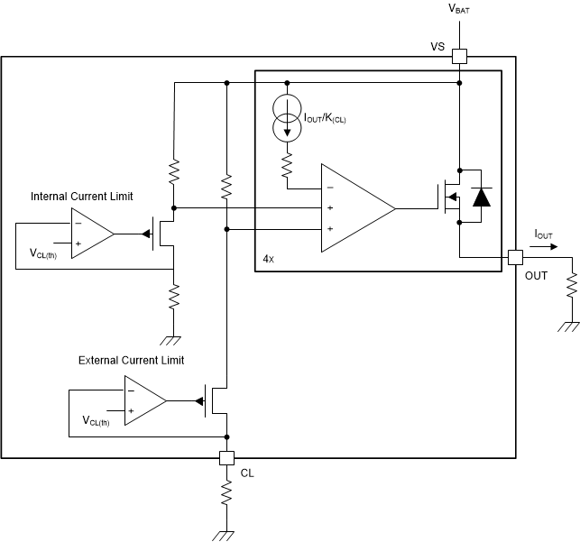
When a current-limit threshold is hit, a closed loop activates immediately. The output current is clamped at the set value, and a fault is reported out. The device heats up due to the high power dissipation on the power FET. If thermal shutdown occurs, the current limit is set to ICL(TSD) to reduce the power dissipation on the power FET. See Figure 23 for more details.
The device has two current-limit thresholds.
- Internal current limit – The internal current limit is fixed at ICL(int). Tie the CL pin directly to the device GND for large-transient-current applications.
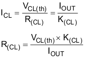
- External adjustable current limit – An external resistor is used to set the current-limit threashold. Use the Equation 4 to calculate the R(CL). VCL(th) is the internal band-gap voltage. K(CL) is the ratio of the output current and the current-limit set value. It is constant across the temperature and supply voltage. The external adjustable current limit allows the flexibility to set the current limit value by applications.

 Figure 23. Current-Limit Block Diargam
 Note that if using a GND network which causes a level shift between the device GND and board GND, the CL pin must be connected with device GND.
For better protection from a hard short-to-GND condition (when the INx pins are enabled, a short to GND occurs suddenly), the device implements a fast-trip protection to turn off the related channel before the current-limit closed loop is set up. The fast-trip response time is less than 1 μs, typically. With this fast response, the device can achieve better inrush current-suppression performance.