SLUS670C JULY 2005 – January 2015 TPS51120
PRODUCTION DATA.
- 1 Features
- 2 Applications
- 3 Description
- 4 Revision History
- 5 Pin Configuration and Functions
- 6 Specifications
-
7 Detailed Description
- 7.1 Overview
- 7.2 Functional Block Diagram
- 7.3
Feature Description
- 7.3.1 PWM Operation
- 7.3.2 Adaptive On-Time Control
- 7.3.3 Light Load Operation
- 7.3.4 Forced PWM Operation
- 7.3.5 5-V, 100-mA, LDO and Switchover (VREG5)
- 7.3.6 3.3-V, 100-mA, LDO and Switchover (VREG3)
- 7.3.7 2-V, 50-uA Sink - Source Reference (VREF2)
- 7.3.8 Low-Side Driver
- 7.3.9 High-Side Driver
- 7.3.10 Soft-Start
- 7.3.11 Soft-Stop
- 7.3.12 Powergood
- 7.3.13 Current Sensing and Overcurrent Protection
- 7.3.14 Overvoltage Protection
- 7.3.15 Undervoltage Protection
- 7.3.16 5-V Supply and UVLO Protection
- 7.3.17 VIN Line Sag Protection (Dynamic UVP)
- 7.3.18 Thermal Shutdown
- 7.4 Device Functional Modes
- 7.5 Programming
- 8 Application and Implementation
- 9 Power Supply Recommendations
- 10Layout
- 11Device and Documentation Support
- 12Mechanical, Packaging, and Orderable Information
Package Options
Refer to the PDF data sheet for device specific package drawings
Mechanical Data (Package|Pins)
- RHB|32
Thermal pad, mechanical data (Package|Pins)
- RHB|32
Orderable Information
5 Pin Configuration and Functions
RHB Package
32-Pin VQFN
Bottom View
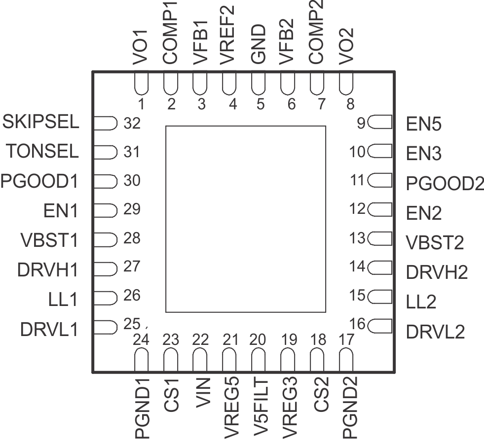
Pin Functions
| PIN | I/O | DESCRIPTION | |
|---|---|---|---|
| NAME | NO. | ||
| COMP1 | 2 | O | Loop compensation pin (error amplifier output). Connect RC from this pin to GND for proper loop compensation with current mode operation. Tie this pin to V5FILT for D-CAP mode operation. |
| COMP2 | 7 | O | |
| CS1 | 23 | I | Current sense comparator input (-) for resistor sensing scheme. Or, overcurrent trip setting input for RDS(on) current sense scheme if connected to V5FILT through the threshold setting resistor. |
| CS2 | 18 | I | |
| DRVH1 | 27 | O | High-side MOSFET gate drive output. Source 3.5 Ω, sink 1.5 Ω, LL-node referenced floating driver. Drive voltage corresponds to VBST to LL voltage. |
| DRVH2 | 14 | O | |
| DRVL1 | 25 | O | Rectifying (low-side) MOSFET gate drive output. Source 3.5 Ω, sink 1.5 Ω, PGND referenced driver. Drive voltage is VREG5 voltage. |
| DRVL2 | 16 | O | |
| EN1 | 29 | I | Channel 1 and Channel 2 SMPS enable pins. Connect to 5 V to turn on with internal 3-ms soft-start. Slower soft-start is possible by applying an external capacitor from each of these pins to ground to program ramp rate. |
| EN2 | 12 | I | |
| EN3 | 10 | I | VREG3, 3.3-V low dropout linear regulator enable pin. Connect to GND to disable. Float or tie to enabled VREG5 to turn on the regulator. |
| EN5 | 9 | I | VREG5, 5-V low dropout linear regulator enable pin. Connect to GND to disable. Float or tie to VBAT to turn on the regulator. |
| GND | 5 | I | Signal ground pin. |
| LL1 | 26 | I/O | High-side MOSFET gate driver return. Also serve as current sense comparator input (-) for RDS(on) sensing, and input voltage monitor for on-time control circuitry |
| LL2 | 15 | I/O | |
| PGND1 | 24 | I/O | Ground return for rectifying MOSFET gate driver. Connect PGND2, PGND1 and GND strongly together near the source of the rectifying FET or the GND connection of the current sense resistor. Also serve as current sense comparator input (+). |
| PGND2 | 17 | I/O | |
| PGOOD1 | 30 | O | Power-good window comparator open drain output. Pull up with resistor to V5FILT or appropriate signal voltage. Current capability is 5-mA. PGOOD goes high 1-ms after VFB is within specified limits. Power bad (terminal goes low) is within 10 μs. |
| PGOOD2 | 11 | O | |
| SKIPSEL | 32 | I | Skip and fault mode selection pin. Refer to Table 5 |
| TONSEL | 31 | I | On-time selection pin. Refer to Table 1 and Table 5. |
| V5FILT | 20 | I | 5-V supply input for the entire control circuit. Should be provided from VREG5 via RC filter. |
| VBST1 | 28 | I | Supply Input for High-side MOSFET Driver. Connect capacitor from this pin to respective LL terminal. An internal PN diode is connected between VREG5 to each of these pins. User can add external schottky diode if forward drop is critical to drive the power MOSFET. |
| VBST2 | 13 | I | |
| VFB1 | 3 | I | SMPS feedback input. Connect the feedback resistor divider here for adjustable outputs. Tie these pins to V5FILT or for fixed output option. Refer to Table 5 |
| VFB2 | 6 | I | |
| VIN | 22 | I | Supply Input for 5-V and 3.3-V linear regulator. Typically connected to VBAT. |
| VO1 | 1 | I | These terminals serve four functions: on-time adjustment, output discharge, VREG5, VREG3 switchover input and feedback inputs for 5-V, 3.3-V fixed-output option. Connect to positive terminal of respective switch mode power supply’s output capacitor. |
| VO2 | 8 | I | |
| VREF2 | 4 | O | 2-V reference output. Capable of ±50-μA, ±2% over 0 - 85°C temperature range. Bypass to GND by 1-nF ceramic capacitor. Tie this pin to GND disables both SMPS. |
| VREG3 | 19 | O | 3.3-V, 100-mA low dropout linear regulator output. Bypass to PGND by 10-μF ceramic capacitor. Runs from VIN supply. Shuts off with EN3. Switches over to VO2 when 3.1 V or above is provided. |
| VREG5 | 21 | O | 5-V, 100-mA low dropout linear regulator output. Bypass to PGND by 10-μF ceramic capacitor. Runs from VIN supply. Internally connected to VBST and DRVL. Shuts off with EN5. Switches over to VO1 when 4.8 V or above is provided. |