SLUS786H OCTOBER 2007 – January 2015 TPS51125
PRODUCTION DATA.
- 1 Features
- 2 Applications
- 3 Description
- 4 Revision History
- 5 Pin Configuration and Functions
- 6 Specifications
-
7 Detailed Description
- 7.1 Overview
- 7.2 Functional Block Diagram
- 7.3
Feature Description
- 7.3.1 PWM Operations
- 7.3.2 Adaptive On-Time Control and PWM Frequency
- 7.3.3 Loop Compensation
- 7.3.4 Ramp Signal
- 7.3.5 Light-Load Condition in Auto-Skip Operation
- 7.3.6 Out-of-Audio Light-Load Operation
- 7.3.7 VREG5/VREG3 Linear Regulators
- 7.3.8 VREG5 Switch Over
- 7.3.9 VREG3 Switch Over
- 7.3.10 Powergood
- 7.3.11 Output Discharge Control
- 7.3.12 Low-Side Driver
- 7.3.13 High-Side Driver
- 7.3.14 VCLK for Charge Pump
- 7.3.15 Current Protection
- 7.3.16 Overvoltage and Undervoltage Protection
- 7.3.17 UVLO Protection
- 7.3.18 Thermal Shutdown
- 7.4 Device Functional Modes
- 8 Application and Implementation
- 9 Power Supply Recommendations
- 10Layout
- 11Device and Documentation Support
- 12Mechanical, Packaging, and Orderable Information
Package Options
Mechanical Data (Package|Pins)
- RGE|24
Thermal pad, mechanical data (Package|Pins)
- RGE|24
Orderable Information
1 Features
- Wide Input Voltage Range: 5.5 V to 28 V
- Output Voltage Range: 2 V to 5.5 V
- Built-In 100-mA, 5-V and 3.3-V LDO With Switches
- Built-In 1% 2-V Reference Output
- With or Without Out-of-Audio™ Mode Selectable Light-Load and PWM-Only Operation
- Internal 1.6-ms Voltage Servo Soft-Start
- Adaptive On-Time Control Architecture With Four Selectable Frequency Setting
- 4500 ppm/°C RDS(on) Current Sensing
- Built-In Output Discharge
- Powergood Output
- Built-In OVP/UVP/OCP
- Thermal Shutdown (Nonlatch)
- QFN, 24-Pin (RGE)
2 Applications
- Notebook Computers
- I/O Supplies
- System Power Supplies
3 Description
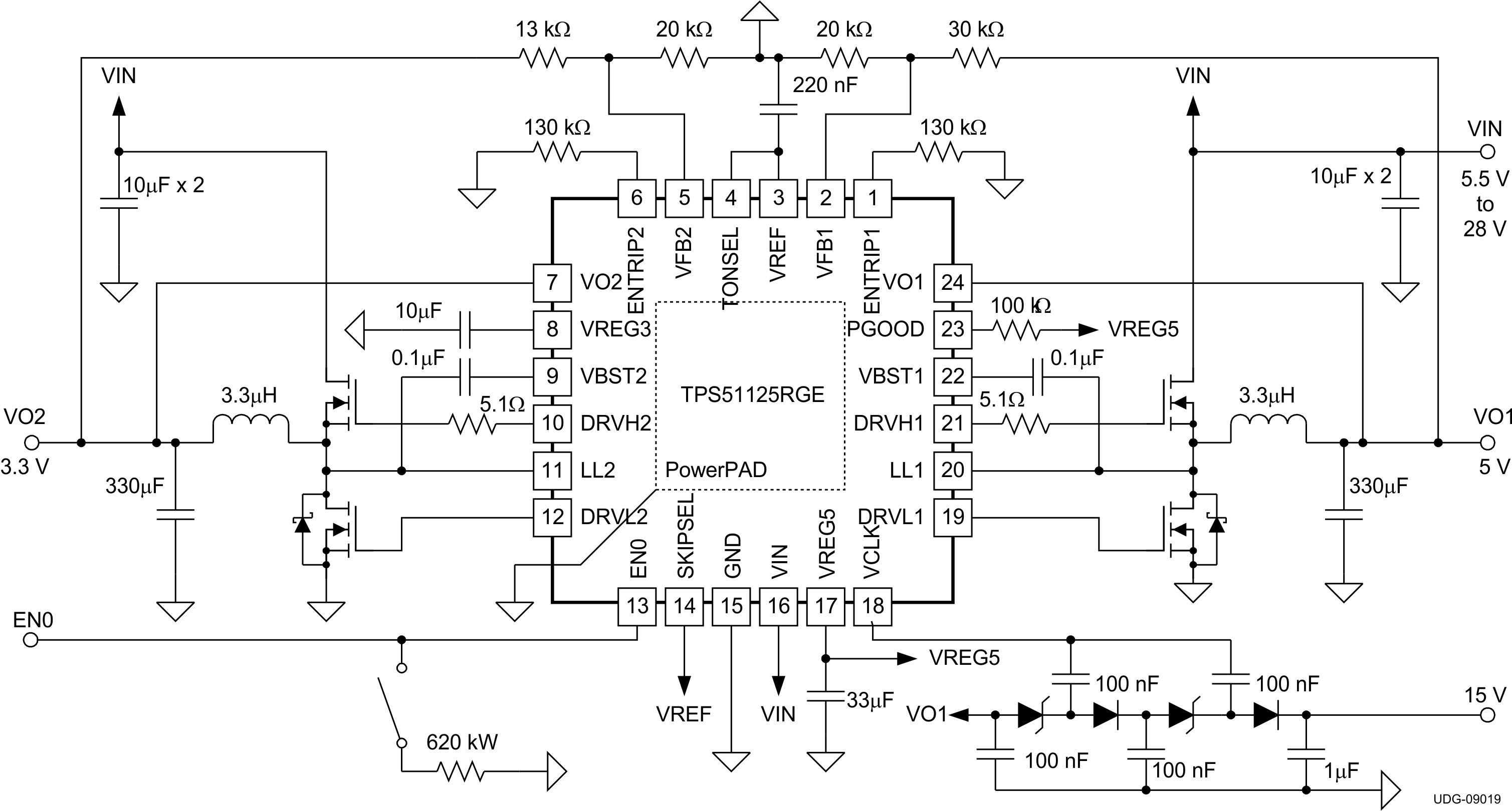
The TPS51125 is a cost-effective, dual-synchronous buck controller targeted for notebook system power supply solutions. The device provides 5-V and 3.3-V LDOs and requires few external components. The 270-kHz VCLK output can be used to drive an external charge pump, thus generating gate drive voltage for the load switches without reducing the efficiency of the main converter. The TPS51125 supports high-efficiency, fast-transient response and provides a combined power-good signal. Out-of-Audio mode light-load operation enables low acoustic noise at much higher efficiency than conventional forced PWM operation. Adaptive on-time D-CAP™ control provides convenient and efficient operation. The part operates with supply input voltages ranging from 5.5 V to 28 V and supports output voltages from 2 V to 5.5 V. The TPS51125 is available in a 24-pin QFN package and is specified from -40°C to 85°C ambient temperature range.
Device Information(1)
| PART NUMBER | PACKAGE | BODY SIZE (NOM) |
|---|---|---|
| TPS51125 | VQFN (24) | 4.00 mm x 4.00 mm |
- For all available packages, see the orderable addendum at the end of the datasheet.
Simplified Schematic