SLUS786H OCTOBER 2007 – January 2015 TPS51125
PRODUCTION DATA.
- 1 Features
- 2 Applications
- 3 Description
- 4 Revision History
- 5 Pin Configuration and Functions
- 6 Specifications
-
7 Detailed Description
- 7.1 Overview
- 7.2 Functional Block Diagram
- 7.3
Feature Description
- 7.3.1 PWM Operations
- 7.3.2 Adaptive On-Time Control and PWM Frequency
- 7.3.3 Loop Compensation
- 7.3.4 Ramp Signal
- 7.3.5 Light-Load Condition in Auto-Skip Operation
- 7.3.6 Out-of-Audio Light-Load Operation
- 7.3.7 VREG5/VREG3 Linear Regulators
- 7.3.8 VREG5 Switch Over
- 7.3.9 VREG3 Switch Over
- 7.3.10 Powergood
- 7.3.11 Output Discharge Control
- 7.3.12 Low-Side Driver
- 7.3.13 High-Side Driver
- 7.3.14 VCLK for Charge Pump
- 7.3.15 Current Protection
- 7.3.16 Overvoltage and Undervoltage Protection
- 7.3.17 UVLO Protection
- 7.3.18 Thermal Shutdown
- 7.4 Device Functional Modes
- 8 Application and Implementation
- 9 Power Supply Recommendations
- 10Layout
- 11Device and Documentation Support
- 12Mechanical, Packaging, and Orderable Information
Package Options
Mechanical Data (Package|Pins)
- RGE|24
Thermal pad, mechanical data (Package|Pins)
- RGE|24
Orderable Information
10 Layout
10.1 Layout Guidelines
Consider these points before starting layout work using the TPS51125.
- TPS51125 has only one GND pin and special care of GND trace design makes operation stable, especially when both channels operate. Group GND terminals of output voltage divider of both channels and the VREF capacitor as close as possible, connect them to an inner GND plane with PowerPad, overcurrent setting resistor, EN0 pull-down resistor and EN0 bypass capacitor as shown in the thin GND line of Figure 43. This trace is named Signal Ground (SGND). Group ground terminals of VIN capacitor(s), VOUT capacitor(s) and source of low-side MOSFETs as close as possible, and connect them to another inner GND plane with GND pin of the device, GND terminal of VREG3 and VREG5 capacitors and 15-V charge-pump circuit as shown in the bold GND line of Figure 43. This trace is named Power Ground (PGND). SGND should be connected to PGND at the middle point between ground terminal of VOUT capacitors.
- Inductor, VOUT capacitor(s), VIN capacitor(s) and MOSFETs are the power components and should be placed on one side of the PCB (solder side). Power components of each channel should be at the same distance from the TPS51125. Other small signal parts should be placed on another side (component side). Inner GND planes above should shield and isolate the small signal traces from noisy power lines.
- PCB trace defined as LLx node, which connects to source of high-side MOSFET, drain of low-side MOSFET and high-voltage side of the inductor, should be as short and wide as possible.
- VREG5 requires capacitance of at least 33 μF and VREG3 requires capacitance of at most 10 μF. VREF requires a 220-nF ceramic bypass capacitor which should be placed close to the device and traces should be no longer than 10 mm.
- Connect the overcurrent setting resistors from ENTRIPx to SGND and close to the device, right next to the device if possible.
- The discharge path (VOx) should have a dedicated trace to the output capacitor; separate from the output voltage sensing trace. When LDO5 is switched over Vo1 trace should be 1.5 mm with no loops. When LDO3 is switched over and loaded Vo2 trace should also be 1.5 mm with no loops. There is no restriction for just monitoring Vox. Make the feedback current setting resistor (the resistor between VFBx to SGND) close to the device. Place on the component side and avoid vias between this resistor and the device.
- Connections from the drivers to the respective gate of the high-side or the low-side MOSFET should be as short as possible to reduce stray inductance. Use 0.65-mm (25 mils) or wider trace and via(s) of at least 0.5 mm (20 mils) diameter along this trace.
- All sensitive analog traces and components such as VOx, VFBx, VREF, GND, EN0, ENTRIPx, PGOOD, TONSEL and SKIPSEL should be placed away from high-voltage switching nodes such as LLx, DRVLx, DRVHx and VCLK nodes to avoid coupling.
- Traces for VFB1 and VFB2 should be short and laid apart each other to avoid channel to channel interference.
- In order to effectively remove heat from the package, prepare thermal land and solder to the package’s thermal pad. Three by three or more vias with a 0.33-mm (13 mils) diameter connected from the thermal land to the internal ground plane should be used to help dissipation. This thermal land underneath the package should be connected to SGND, and should NOT be connected to PGND.
10.2 Layout Example
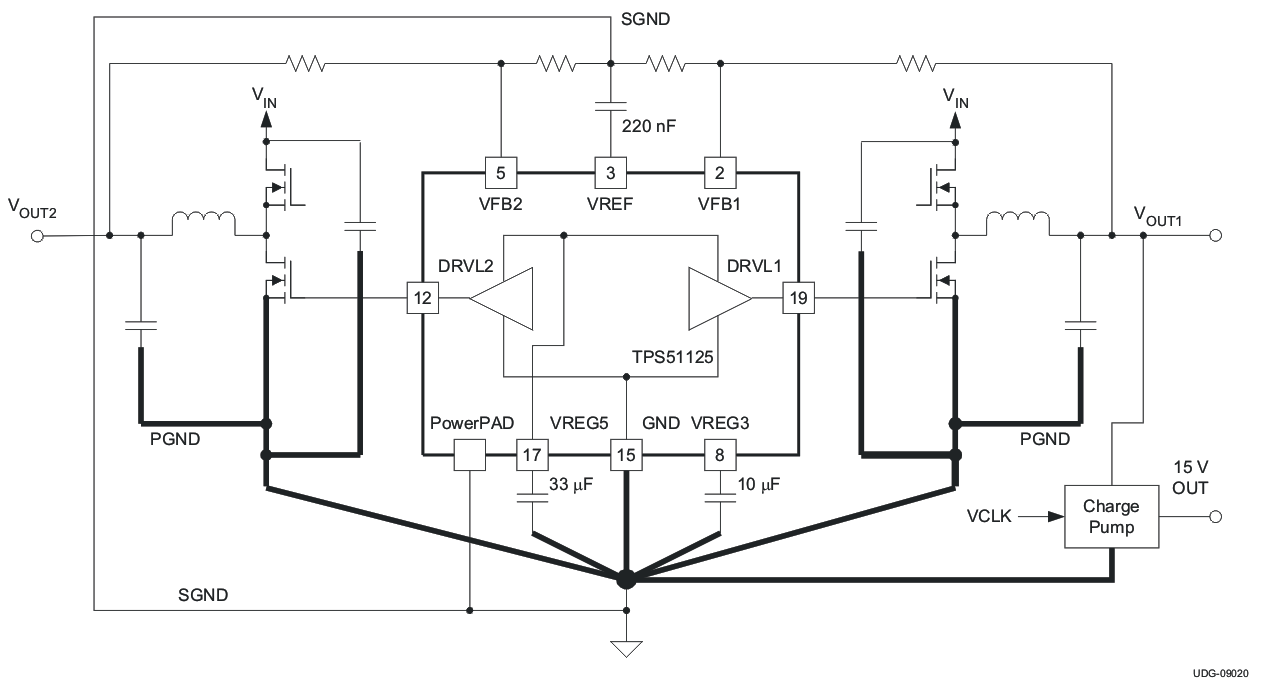 Figure 43. Ground System
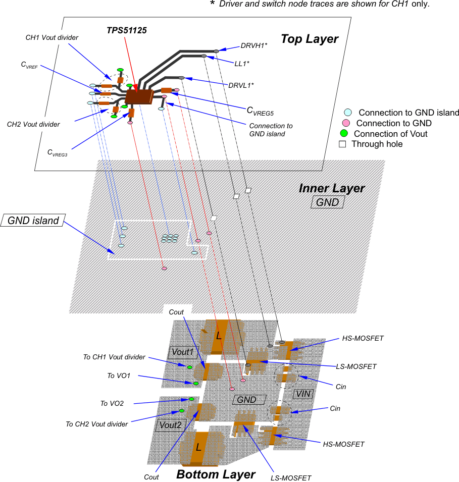 Figure 44. PCB Layout