SLUSB94A OCTOBER 2012 – September 2016 TPS51716
PRODUCTION DATA.
- 1 Features
- 2 Applications
- 3 Description
- 4 Revision History
- 5 Pin Configuration and Functions
- 6 Specifications
-
7 Detailed Description
- 7.1 Overview
- 7.2 Functional Block Diagram
- 7.3
Feature Description
- 7.3.1 VDDQ Switch Mode Power Supply Control
- 7.3.2 VREF and REFIN, VDDQ Output Voltage
- 7.3.3 Soft-Start and Powergood
- 7.3.4 Power State Control
- 7.3.5 VDDQ Overvoltage and Undervoltage Protection
- 7.3.6 VDDQ Out-of-Bound Operation
- 7.3.7 VDDQ Overcurrent Protection
- 7.3.8 VTT and VTTREF
- 7.3.9 VTT Overcurrent Protection
- 7.3.10 V5IN Undervoltage Lockout (UVLO) Protection
- 7.3.11 Thermal Shutdown
- 7.4 Device Functional Modes
- 8 Application and Implementation
- 9 Power Supply Recommendations
- 10Layout
- 11Device and Documentation Support
- 12Mechanical, Packaging, and Orderable Information
Package Options
Mechanical Data (Package|Pins)
- RUK|20
Thermal pad, mechanical data (Package|Pins)
- RUK|20
Orderable Information
8 Application and Implementation
NOTE
Information in the following applications sections is not part of the TI component specification, and TI does not warrant its accuracy or completeness. TI’s customers are responsible for determining suitability of components for their purposes. Customers should validate and test their design implementation to confirm system functionality.
8.1 Application Information
TPS51716 is typically used as step down converters, which converts a voltage from 3V- 28V to 0.7 V to 1.8 V output voltage and provide a total solution to memory system.
8.2 Typical Application
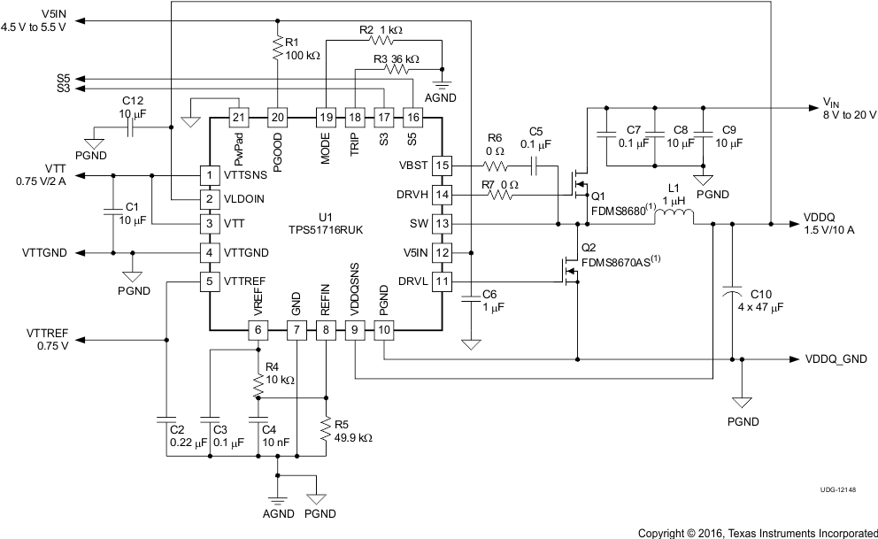
Table 3. DDR3, DCAP-2 500-kHz Application Circuit, List of Materials
| REFERENCE DESIGNATOR | QTY | SPECIFICATION | MANUFACTURE | PART NUMBER |
|---|---|---|---|---|
| C8, C9 | 2 | 10 µF, 25 V | Taiyo Yuden | TMK325BJ106MM |
| C10 | 4 | 47 µF, 6.3 V | TDK | C2012X5R0J476M |
| L1 | 1 | 1 µH, 18.5 A, 2.3 mΩ | NEC Tokin | MPC1055L1R0C |
| Q1 | 1 | 30 V, 35 A, 8.5 mΩ | Fairchild | FDMS8680 |
| Q2 | 1 | 30 V, 42 A, 3.5 mΩ | Fairchild | FDMS8670AS |
8.2.1 Design Requirements
To begin the design process, the user must know a few application parameters (see Table 4).
Table 4. Design Parameters
| PARAMETER | EXAMPLE VALUE |
|---|---|
| Input voltage range | 8 to 20 V |
| Output voltage | 1. 5 V |
| Transient response, 1.5-A load step | ΔVout = ±5% |
| Input ripple voltage | 400 mV |
| Output ripple voltage | 40 mV |
| Output current rating | 10A |
| Operating frequency | 670 kHz/ 500 kHz |
8.2.2 Detailed Design Procedure
The following design procedure can be used to select component values for the TPS51716.
8.2.2.1 External Components Selection
The external components selection is a simple process.
- Determine the value of R1 and R2
- Choose the inductor
- Choose the OCL setting resistance, RTRIP
- Choose the output capacitors
- RC × CC time constant is 23 µs for 500 kHz operation (or 14.6 µs for 670-kHz operation)
- G = 0.25
The output voltage is determined by the value of the voltage-divider resistor, R1 and R2. R1 is connected between VREF and REFIN pins, and R2 is connected between the REFIN pin and GND. Setting R1 to 10-kΩ is a good starting point. Determine R2 using Equation 5.
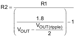
For an application using organic semiconductor capacitor(s) or specialty polymer capacitor(s) for the output capacitor(s), the output voltage ripple can be calculated as shown in Equation 6.

For an application using ceramic capacitor(s) as the output capacitor(s), the output voltage ripple can be calculated as shown in Equation 7.

The inductance value should be determined to yield a ripple current of approximately ¼ to ½ of maximum output current. Larger ripple current increases output ripple voltage and improves the signal-to-noise ratio and helps stable operation.

The inductor needs a low direct current resistance (DCR) to achieve good efficiency, as well as enough room above peak inductor current before saturation. The peak inductor current can be estimated in Equation 9.

Combining Equation 1 and Equation 2, RTRIP can be obtained using Equation 10.

Determine output capacitance to meet small signal stability as shown in Equation 11.

where
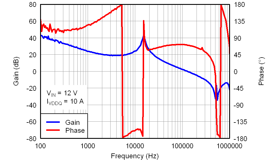
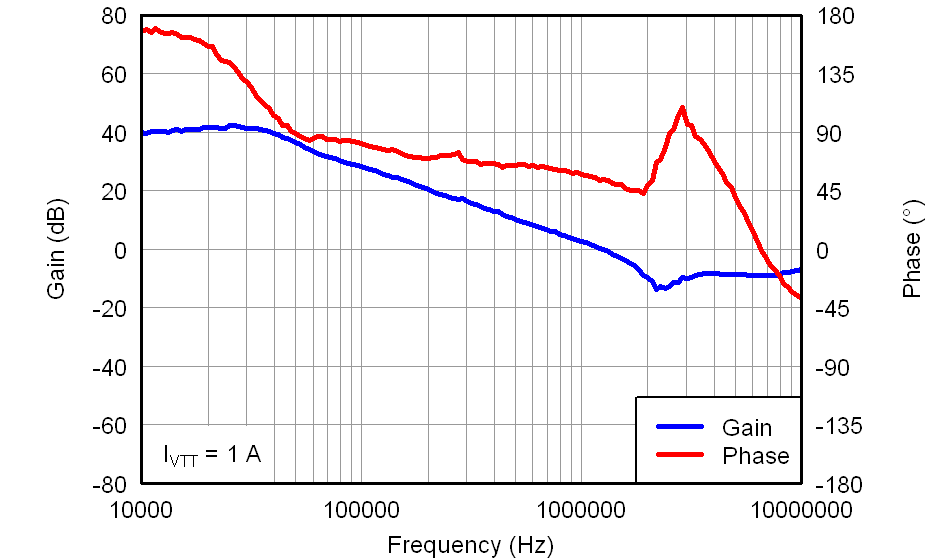
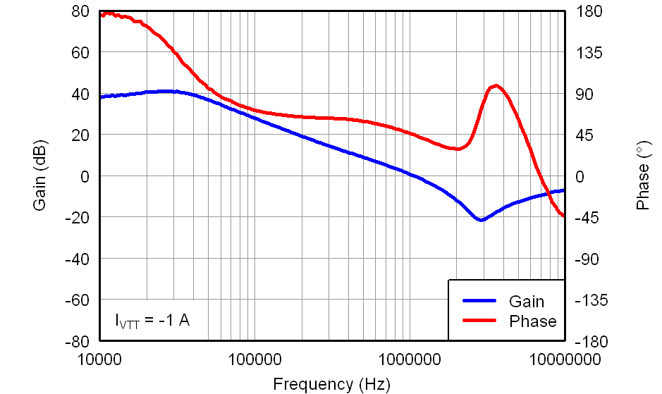
8.2.3 Application Curves
