SLUSAS8A December 2011 – October 2016 TPS53313
PRODUCTION DATA.
- 1 Features
- 2 Applications
- 3 Description
- 4 Revision History
- 5 Pin Configuration and Functions
- 6 Specifications
- 7 Detailed Description
- 8 Application and Implementation
- 9 Power Supply Recommendations
- 10Layout
- 11Device and Documentation Support
- 12Mechanical, Packaging, and Orderable Information
Package Options
Mechanical Data (Package|Pins)
- RGE|24
Thermal pad, mechanical data (Package|Pins)
- RGE|24
Orderable Information
7 Detailed Description
7.1 Overview
The TPS53313 is a high-efficiency switching regulator with two integrated N-channel MOSFETs and is capable of delivering up to 6 A of load current. The TPS53316 provides output voltage from 0.6 V up to 0.7 × VIN from
4.5-V to 16-V wide input voltage range. The output voltage accuracy is better than ±1% over load, line, and temperature.
This device can operate in either forced continuous conduction mode (FCCM) or skip mode with selectable soft-start time to fit various application needs. Skip mode operation provides reduced power loss and increases the efficiency at light load. The unique, patented PWM modulator enables smooth light load to heavy load transition while maintaining fast load transient.
7.2 Functional Block Diagram

7.3 Feature Description
7.3.1 Soft-Start Operation
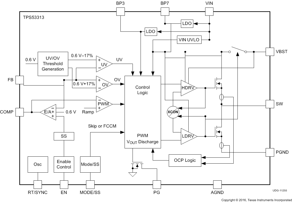
The soft-start operation reduces the inrush current during the start-up time. A slow rising reference is generated by the soft-start circuitry and sent to the input of the error amplifier. When the soft-start ramp voltage is less than 600 mV, the error amplifier uses this ramp voltage as the reference. When the ramp voltage reaches 600 mV, a fixed 600-mV reference voltage is used for the error amplifier. The soft-start time has selectable values of 1 ms, 3 ms, and 6 ms.
7.3.2 Power Good
The TPS53313 monitors the output voltage through the FB pin. If the FB voltage is within 117% and 83% of the reference voltage, the power good signal remains high. If the FB voltage is outside of this range, the PG pin pin is pulled low by the internal open drain output.
During start up, the power good signal has a 200-µs delay after the FB voltage falls into the power good range limit when the soft-start time is set to 1 ms. There is also 10-µs delay during shut down.
7.3.3 UVLO Function
The TPS53313 provides UVLO protection for input voltage, VIN. If the input voltage is lower than UVLO threshold voltage minus the hysteresis, the device shut off. When the voltage rises above the threshold voltage, the device restarts. The typical UVLO rising threshold is 4.23 V. Hysteresis of 200 mV for input voltage is provided to prevent glitch.
7.3.4 Overcurrent (OC) Protection
The TPS53313 provides peak current protection and continuously monitors the current flowing through high-side and low-side MOSFETs. If the current through the high-side FET exceeds the current limit threshold, the high-side FET turns off and the low-side FET turns on. An overcurrent (OC) counter starts to increment every switching cycle to count the occurrence of the overcurrent events. The converter shuts down immediately when the OC counter reaches 4. The OC counter resets if the detected current is less than 6 A (with 6-A OC setting) after an OC event.
Another set of overcurrent circuitry monitors the current through low-side FET. If the current through the low-side FET exceeds 6 A (with 6-A OC setting), the overcurrent protection is engaged and turns off both high-side and low-side FETs immediately.
Therefore, the device is fully protected against overcurrent during both on-time and off-time. Also, the OC threshold is selectable and can be set to 4.5 A, 6 A, or 9 A by connecting different capacitor in parallel with MODE/SS pin. After OC events, the device stops switching and enters hiccup mode. A re-start is attempted after a hiccup waiting time. If the fault condition is not cleared, hiccup mode operation may continue indefinitely
7.3.5 Overvoltage and Undervoltage Protection
The TPS53313 monitors the voltage divided feedback voltage to detect the overvoltage and undervoltage conditions. When the feedback voltage is greater than 117% of the reference, overvoltage protection is triggered, the high-side MOSFET turns off and the low-side MOSFET turns on. Then the output voltage drops and the FB voltage reaches the undervoltage threshold. At that point the low-side MOSFET turns off and the device goes into tri-state logic.
When the feedback voltage is lower than 83% of the reference voltage, the undervoltage protection counter starts. If the feedback voltage remains lower than the undervoltage threshold voltage after 10 µs, the device turns off both the high-side and low-side MOSFETs and then goes into tri-state logic.
After the undervoltage events, the device stops switching and enters hiccup mode. A restart is attempted after a hiccup waiting time. If the fault condition is not cleared, hiccup mode operation may continue indefinitely.
7.3.6 Overtemperature Protection
The TPS53313 continuously monitors the die temperature. If the die temperature exceeds the threshold value (140°C typical), the device shuts off. When the device is cooled to 40°C below the overtemperature threshold, it restarts and returns to normal operation.
7.3.7 Output Discharge
When the EN pin is low, the TPS53313 discharges the output capacitors through an internal MOSFET switch between SW and GND while the high-side and low-side MOSFETs are maintained in the OFF state. The typical discharge switch on resistance is 120 Ω. This function is disabled when VVIN is less than 1 V.
7.3.8 Switching Frequency Setting and Synchronization
The clock frequency is programmed by the value of the resistor connected from the RT/SYNC pin to GND. The switching frequency is programmable between 250 kHz and 1.5 MHz.
Also, TPS53313 is able to synchronize to external clock. The synchronization is fulfilled by connecting the RT/SYNC pin to external clock source. If no external pulse is received from RT/SYNC pin, the device continues to operate the internal clock.
7.4 Device Functional Modes
7.4.1 Operation Mode
The TPS53313 has 6 operation modes determined by the MODE/SS pin connection as listed in Table 1. The current limit thresholds and associated capacitance selections are shown in Table 2.
Table 1. Operation Mode Selection
| MODE/SS PIN CONNECTION | OPERATION MODE | tSS SOFT-START TIME (ms) |
|---|---|---|
| 10 kΩ to GND | FCCM | 6 |
| 20 kΩ to GND | FCCM | 3 |
| 39 kΩ to GND | FCCM | 1 |
| 82 kΩ to GND | Skip mode | 6 |
| 160 kΩ to GND | Skip mode | 3 |
| Floating | Skip mode | 1 |
Table 2. Capacitor Selection
| MODE/SS PIN SETTING (nF) | CURRENT LIMIT THRESHOLD (A) |
|---|---|
| No capacitor | 6 |
| 2.2 | 4.5 |
| 10 | 9 |
In forced continuous conduction mode (FCCM), the high-side FET is ON during the on-time and low-side FET is ON during the off-time. The switching is synchronized to the internal clock thus the switching frequency is fixed.
In this mode, the switching frequency remains constant over the entire load range which is suitable for applications that need tight control of switching frequency.
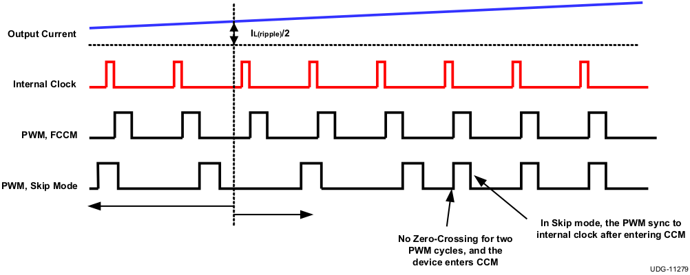
In skip mode, the high-side FET is on during the on-time and low-side FET is on during the off-time until the inductor current reaches zero. An internal zero-crossing comparator detects the zero crossing of inductor current from positive to negative. When the inductor current reaches zero, the comparator sends a signal to the logic control and turns off the low-side FET. The on-pulse in skip mode is designed to be 25% higher than CCM to provide hysteresis to avoid chattering between CCM and skip mode.
Also, the overcurrent protection threshold can be set to 4.5 A, 6 A or 9 A by changing the capacitor that is in parallel with MODE/SS pin. Specifically, a 6-A current limit threshold is set without an external capacitor, the 4.5 A current limit threshold is set with a 2.2-nF capacitor, and the 9-A current limit threshold is set when a 10-nF capacitor is in parallel with MODE/SS pin.
7.4.2 Light Load Operation
In skip mode, when the load current is less than half of inductor ripple current, the inductor current reaches zero by the end of OFF-Time. The light load control scheme then turns off the low-side MOSFET when inductor current reaches zero. Since there is no negative inductor current, the energy delivered to the load per switching cycle is increased compared to the normal PWM mode operation. The controller then reduces the switching frequency to maintain the output voltage regulation. The switching loss is reduced and thus efficiency is improved.
In skip mode, when the load current decreases, the switching frequency also decreases continuously in discontinuous conduction mode (DCM). When the load current is 0 A, the minimum switching frequency is reached. It is also required that the difference between VVBST and VSW to be higher than 3.3 V to ensure the supply for high-side gate driver.
 Figure 12. TPS53313 Operation Modes in Light and Heavy Load Conditions
7.4.3 Forced Continuous Conduction Mode
When choosing FCCM, the TPS53313 is operating in continuous conduction mode in both light and heavy load condition. In this mode, the switching frequency remains constant over the entire load range which is suitable for applications need tight control of switching frequency at a cost of lower efficiency at light load.