SLUSBG4B March   2013  – August 2021 TPS53511

PRODUCTION DATA  

  1. Features
  2. Applications
  3. Description
  4. Revision History
  5. Pin Configuration and Functions
  6. Specifications
    1. 6.1 Absolute Maximum Ratings
    2. 6.2 ESD Ratings
    3. 6.3 Recommended Operating Conditions
    4. 6.4 Thermal Information
    5. 6.5 Electrical Characteristics
    6. 6.6 Typical Characteristics
  7. Detailed Description
    1. 7.1 Overview
    2. 7.2 Functional Block Diagram
    3. 7.3 Feature Description
      1. 7.3.1 PWM Operation
      2. 7.3.2 PWM Frequency and Adaptive On-Time Control
      3. 7.3.3 Soft Start and Pre-Biased Soft-Start Function
      4. 7.3.4 Power Good
      5. 7.3.5 Output Discharge Control
      6. 7.3.6 Current Protection
      7. 7.3.7 Overvoltage/Undervoltage Protection
      8. 7.3.8 UVLO Protection
      9. 7.3.9 Thermal Shutdown
    4. 7.4 Device Functional Modes
      1. 7.4.1 Light Load Mode Control
  8. Application and Implementation
    1. 8.1 Application Information
    2. 8.2 Typical Application
      1. 8.2.1 Design Requirements
      2. 8.2.2 Detailed Design Procedure
        1. 8.2.2.1 Output Inductor Selection
        2. 8.2.2.2 Output Capacitor Selection
        3. 8.2.2.3 Input Capacitor Selection
        4. 8.2.2.4 Bootstrap Capacitor Selection
        5. 8.2.2.5 VREG5 Capacitor Selection
        6. 8.2.2.6 Output Voltage Setting Resistors Selection
      3. 8.2.3 Application Curves
  9. Power Supply Recommendations
  10. 10Layout
    1. 10.1 Layout Considerations
      1. 10.1.1 Thermal Information
    2. 10.2 Layout Example
  11. 11Device and Documentation Support
    1. 11.1 Device Support
      1. 11.1.1 Third-Party Products Disclaimer
    2. 11.2 Receiving Notification of Documentation Updates
    3. 11.3 Support Resources
    4. 11.4 Trademarks
    5. 11.5 Electrostatic Discharge Caution
    6. 11.6 Glossary
  12. 12Mechanical, Packaging, and Orderable Information

Package Options

Mechanical Data (Package|Pins)
Thermal pad, mechanical data (Package|Pins)
Orderable Information

Output Voltage Setting Resistors Selection

The output voltage is set with a resistor divider from the output node to the VFB pin. It is recommended to use 1% tolerance or better divider resistors. Begin by using Equation 7 and Equation 8 to calculate VOUT.

To improve efficiency at light-load condition, use resistors with a relatively larger value. However, too high resistance value make the circuit more susceptible to noise, and voltage errors from the VFB input current is more noticeable.

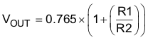
For output voltages from 0.76 V to 2.5 V:

Equation 7. GUID-08A5DCA6-E1F0-4605-A85E-24DAFD65878B-low.gif

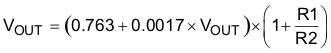
For output voltages over 2.5 V:

Equation 8. GUID-7467BED2-3742-49E9-A1E9-20470B8095EA-low.gif

The required output voltage for this design is 1.05 V. So Equation 7 is used to calculate the value of R1. R2 is 22.1 kΩ, therefore, R1 is 8.25 kΩ.