SLVSB56C May 2012 – February 2014 TPS54160 , TPS54160A
PRODUCTION DATA.
- 1 Features
- 2 Applications
- 3 Description
- 4 Simplified Schematic
- 5 Revision History
- 6 Terminal Configuration and Functions
- 7 Specifications
-
8 Detailed Description
- 8.1 Overview
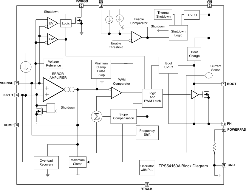
- 8.2 Functional Block Diagram
- 8.3
Feature Description
- 8.3.1 Fixed Frequency PWM Control
- 8.3.2 Slope Compensation Output Current
- 8.3.3 Pulse Skip Eco-mode
- 8.3.4 Bootstrap Voltage (BOOT)
- 8.3.5 Low Dropout Operation
- 8.3.6 Error Amplifier
- 8.3.7 Voltage Reference
- 8.3.8 Adjusting the Output Voltage
- 8.3.9 Enable and Adjusting Undervoltage Lockout
- 8.3.10 Slow Start and Tracking Pin (SS/TR)
- 8.3.11 Overload Recovery Circuit
- 8.3.12 Sequencing
- 8.3.13 Constant Switching Frequency and Timing Resistor (RT/CLK Pin)
- 8.3.14 Overcurrent Protection and Frequency Shift
- 8.3.15 Selecting the Switching Frequency
- 8.3.16 How to Interface to RT/CLK Pin
- 8.3.17 Power Good (PWRGD Pin)
- 8.3.18 Overvoltage Transient Protection
- 8.3.19 Thermal Shutdown
- 8.3.20 Small Signal Model for Loop Response
- 8.3.21 Simple Small Signal Model for Peak Current Mode Control
- 8.3.22 Small Signal Model for Frequency Compensation
- 8.4 Device Functional Modes
-
9 Application and Implementation
- 9.1 Application Information
- 9.2
Typical Application
- 9.2.1 Design Requirements
- 9.2.2
Detailed Design Procedures
- 9.2.2.1 Selecting the Switching Frequency
- 9.2.2.2 Output Inductor Selection (LO)
- 9.2.2.3 Output Capacitor
- 9.2.2.4 Catch Diode
- 9.2.2.5 Input Capacitor
- 9.2.2.6 Slow Start Capacitor
- 9.2.2.7 Bootstrap Capacitor Selection
- 9.2.2.8 Under Voltage Lock Out Set Point
- 9.2.2.9 Output Voltage and Feedback Resistors Selection
- 9.2.2.10 Compensation
- 9.2.2.11 Power Dissipation Estimate
- 9.2.3 Application Curves
- 10Power Supply Recommendations
- 11Layout
- 12Device and Documentation Support
- 13Mechanical, Packaging, and Orderable Information
Package Options
Mechanical Data (Package|Pins)
- DGQ|10
Thermal pad, mechanical data (Package|Pins)
- DGQ|10
Orderable Information
8 Detailed Description
8.1 Overview
The TPS54160A device is a 60-V, 1.5-A, step-down (buck) regulator with an integrated high-side n-channel MOSFET. To improve performance during line and load transients the device implements a constant frequency, current mode control which reduces output capacitance and simplifies external frequency compensation design. The wide switching frequency of 100kHz to 2500kHz allows for efficiency and size optimization when selecting the output filter components. The switching frequency is adjusted using a resistor to ground on the RT/CLK pin. The device has an internal phase lock loop (PLL) on the RT/CLK pin that is used to synchronize the power switch turn on to a falling edge of an external system clock.
The TPS54160A has a default start up voltage of approximately 2.5V. The EN pin has an internal pull-up current source that can be used to adjust the input voltage under voltage lockout (UVLO) threshold with two external resistors. In addition, the pull up current provides a default condition. When the EN pin is floating the device operates. The operating current is 116 μA when not switching and under no load. When the device is disabled, the supply current is 1.3 μA.
The integrated 200mΩ high-side MOSFET allows for high efficiency power supply designs capable of delivering 1.5 A of continuous current to a load. The TPS54160A reduces the external component count by integrating the boot recharge diode. The bias voltage for the integrated high-side MOSFET is supplied by a capacitor on the BOOT to PH pin. The boot capacitor voltage is monitored by an UVLO circuit and turns on the high-side MOSFET off when the boot voltage falls below a preset threshold. The TPS54160A can operate at high duty cycles because of the boot UVLO. The output voltage can be stepped down to as low as the 0.8V reference.
The TPS54160A has a power good comparator (PWRGD) which asserts when the regulated output voltage is less than 92% or greater than 109% of the nominal output voltage. The PWRGD pin is an open drain output which deasserts when the VSENSE pin voltage is between 94% and 107% of the nominal output voltage allowing the pin to transition high when a pull-up resistor is used.
The TPS54160A minimizes excessive output overvoltage (OV) transients by taking advantage of the OV power good comparator. When the OV comparator is activated, the high-side MOSFET is turned off and masked from turning on until the output voltage is lower than 107%.
The SS/TR (slow start/tracking) pin is used to minimize inrush currents or provide power supply sequencing during power up. A small value capacitor should be coupled to the pin to adjust the slow start time. A resistor divider can be coupled to the pin for critical power supply sequencing requirements. The SS/TR pin is discharged before the output powers up. This discharging ensures a repeatable restart after an over-temperature fault, UVLO fault or a disabled condition.
The TPS54160A, also, discharges the slow start capacitor during overload conditions with an overload recovery circuit. The overload recovery circuit will slow start the output from the fault voltage to the nominal regulation voltage once a fault condition is removed. A frequency foldback circuit reduces the switching frequency during startup and overcurrent fault conditions to help control the inductor current.
8.2 Functional Block Diagram
8.3 Feature Description
8.3.1 Fixed Frequency PWM Control
The TPS54160A uses an adjustable fixed frequency, peak current mode control. The output voltage is compared through external resistors on the VSENSE pin to an internal voltage reference by an error amplifier which drives the COMP pin. An internal oscillator initiates the turn on of the high-side power switch. The error amplifier output is compared to the high-side power switch current. When the power switch current reaches the level set by the COMP voltage, the power switch is turned off. The COMP pin voltage will increase and decrease as the output current increases and decreases. The device implements a current limit by clamping the COMP pin voltage to a maximum level. The Eco-mode™ is implemented with a minimum clamp on the COMP pin.
8.3.2 Slope Compensation Output Current
The TPS54160A adds a compensating ramp to the switch current signal. This slope compensation prevents sub-harmonic oscillations. The available peak inductor current remains constant over the full duty cycle range.
8.3.3 Pulse Skip Eco-mode
The TPS54160A enters the pulse skip mode when the voltage on the COMP pin is the minimum clamp value. The TPS54160A operates in a pulse skip mode at light load currents to improve efficiency. The peak switch current during the pulse skip mode will be the greater value of 50mA or the peak inductor current that is a function of the minimum on time, input voltage, output voltage and inductance value. When the load current is low and the output voltage is within regulation the device will enter a sleep mode and draw only 116 μA input quiescent current. While the device is in sleep mode the output power is delivered by the output capacitor. As the load current decreases, the time the output capacitor supplies the load current increases and the switching frequency decreases reducing gate drive and switching losses. As the output voltage drops, the TPS54160A wakes up from the sleep mode and the power switch turns on to recharge the output capacitor, see Figure 25. The internal PLL remains operating when in sleep mode. When operating at light load currents in the pulse skip mode the switching transitions occur synchronously with the external clock signal.
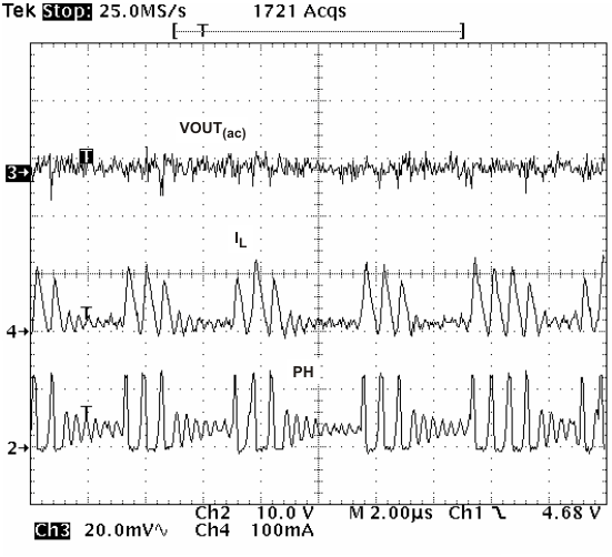 Figure 25. Pulse Skip Mode Operation
8.3.4 Bootstrap Voltage (BOOT)
The TPS54160A has an integrated boot regulator and requires a small ceramic capacitor between the BOOT and PH pin to provide the gate drive voltage for the high side MOSFET. The value of the ceramic capacitor should be 0.1 μF. A ceramic capacitor with an X7R or X5R grade dielectric is recommended because of the stable characteristics over temperature and voltage. To improve drop out, the TPS54160A is designed to operate at 100% duty cycle as long as the BOOT to PH pin voltage is greater than 2.1 V. When the voltage from BOOT to PH drops below 2.1 V, the high side MOSFET is turned off using an UVLO circuit allowing for the low side diode to conduct which allows refreshing of the BOOT capacitor. Since the supply current sourced from the BOOT capacitor is low, the high side MOSFET can remain on for more switching cycles than it refreshes, thus, the effective duty cycle limitation that is attributed to the boot regulator system is high.
8.3.5 Low Dropout Operation
The duty cycle during dropout of the regulator will be mainly determined by the voltage drops across the power MOSFET, inductor, low side diode and printed circuit board resistance. During operating conditions in which the input voltage drops, the high side MOSFET can remain on for 100% of the duty cycle to maintain output regulation or until the BOOT to PH voltage falls below 2.1 V.
Once the high side is off, the low side diode will conduct and the BOOT capacitor will be recharged. During this boot capacitor recharge time, the inductor current will ramp down until the high side MOSFET turns on. The recharge time is longer than the typical high side off time of previous switching cycles, and thus, the inductor current ripple is larger resulting in more ripple voltage on the output. The recharge time is a function of the input voltage, boot capacitor value, and the impedance of the internal boot recharge diode.
Attention needs to be taken in maximum duty cycle applications which experience extended time periods without a load current. When the voltage across the BOOT capacitors falls below the 2.1 V threshold in applications that have a difference in the input voltage and output voltage that is less than 3V, the high side MOSFET will be turned off but there is not enough current in the inductor to pull the PH pin down to recharge the boot capacitor. The regulator will not switch because the boot capacitor is less than 2.1V and the output capacitor will decay until the difference in the input voltage and output voltage is 2.1 V. At this time the boot under voltage lockout is exceeded and the device will switch until the desired output voltage is reached.
The start and stop voltages are shown in Figure 26 and Figure 27. The voltages are plotted versus load current. The start voltage is defined as the input voltage needed to regulate the output within 1%. The stop voltage is defined as the input voltage at which the output drops by 5% or stops switching.
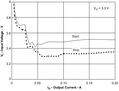 Figure 26. 3.3V Start/Stop Voltage
 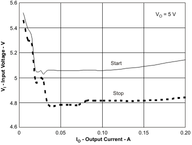 Figure 27. 5.0V Start/Stop Voltage
 8.3.6 Error Amplifier
The TPS54160A has a transconductance amplifier for the error amplifier. The error amplifier compares the VSENSE voltage to the lower of the SS/TR pin voltage or the internal 0.8-V voltage reference. The transconductance (gM) of the error amplifier is 97 μA/V during normal operation. During the slow start operation, the transconductance is a fraction of the normal operating transconductance. When the voltage of the VSENSE pin is below 0.8 V and the device is regulating using the SS/TR voltage, the transconductance is 26 μA/V.
The frequency compensation components (capacitor, series resistor and capacitor) are added to the COMP pin to ground.
8.3.7 Voltage Reference
The voltage reference system produces a precise ±2% voltage reference over temperature by scaling the output of a temperature stable bandgap circuit.
8.3.8 Adjusting the Output Voltage
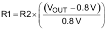
The output voltage is set with a resistor divider from the output node to the VSENSE pin. It is recommended to use 1% tolerance or better divider resistors. Start with a 10 kΩ for the R2 resistor and use the Equation 1 to calculate R1. To improve efficiency at light loads consider using larger value resistors. If the values are too high, the regulator becomes more susceptible to noise and voltage errors from the VSENSE input current are noticeable.
8.3.9 Enable and Adjusting Undervoltage Lockout
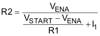
The TPS54160A is disabled when the VIN pin voltage falls below 2.5 V. If an application requires a higher undervoltage lockout (UVLO), use the EN pin as shown in Figure 28 to adjust the input voltage UVLO by using the two external resistors. Though it is not necessary to use the UVLO adjust registers, for operation it is highly recommended to provide consistent power up behavior. The EN pin has an internal pull-up current source, I1, of 0.9μA that provides the default condition of the TPS54160A operating when the EN pin floats. Once the EN pin voltage exceeds 1.25V, an additional 2.9 μA of hysteresis, Ihys, is added. This additional current facilitates input voltage hysteresis. Use Equation 2 to set the external hysteresis for the input voltage. Use Equation 3 to set the input start voltage.
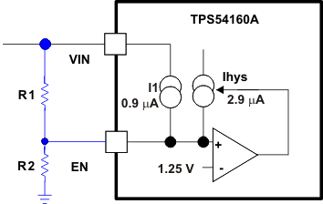 Figure 28. Adjustable Undervoltage Lockout (UVLO)
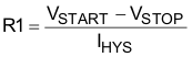
Another technique to add input voltage hysteresis is shown in Figure 29. This method may be used, if the resistance values are high from the previous method and a wider voltage hysteresis is needed. The resistor R3 sources additional hysteresis current into the EN pin.
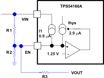 Figure 29. Adding Additional Hysteresis
Do not place a low-impedance voltage source with greater than 5 V directly on the EN pin. Do not place a capacitor directly on the EN pin if VEN > 5 V when using a voltage divider to adjust the start and stop voltage. The node voltage, (see Figure 30) must remain equal to or less than 5.8 V. The zener diode can sink up to 100 µA. The EN pin voltage can be greater than 5 V if the VIN voltage source has a high impedance and does not source more than 100 µA into the EN pin.
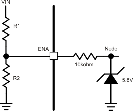 Figure 30. Node Voltage
8.3.10 Slow Start and Tracking Pin (SS/TR)
The TPS54160A effectively uses the lower voltage of the internal voltage reference or the SS/TR pin voltage as the power-supply's reference voltage and regulates the output accordingly. A capacitor on the SS/TR pin to ground implements a slow start time. The TPS54160A has an internal pull-up current source of 2μA that charges the external slow start capacitor. The calculations for the slow start time (10% to 90%) are shown in Equation 6. The voltage reference (VREF) is 0.8 V and the slow start current (ISS) is 2μA. The slow start capacitor should remain lower than 0.47 μF and greater than 0.47 nF.
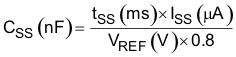
At power up, the TPS54160A does not start switching until the slow start pin is discharged to less than 40 mV to ensure a proper power up, see Figure 31.
Also, during normal operation, the TPS54160A stops switching and the SS/TR must be discharged to 40 mV when the voltage at the VIN pin is below the VIN UVLO, EN pin pulled below 1.25 V, or a thermal shutdown event occurs.
The VSENSE voltage follows the SS/TR pin voltage with a 45 mV offset up to 85% of the internal voltage reference. When the SS/TR voltage is greater than 85% on the internal reference voltage the offset increases as the effective system reference transitions from the SS/TR voltage to the internal voltage reference (see Figure 23). The SS/TR voltage ramps linearly until clamped at 1.7 V.
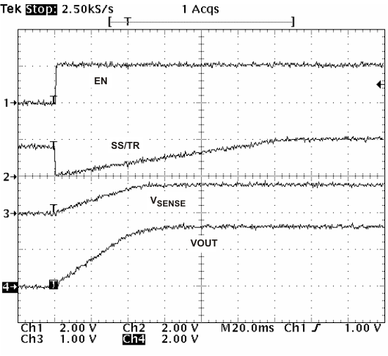 Figure 31. Operation of SS/TR Pin when Starting
8.3.11 Overload Recovery Circuit
The TPS54160A has an overload recovery (OLR) circuit. The OLR circuit slow starts the output from the overload voltage to the nominal regulation voltage once the fault condition is removed. The OLR circuit discharges the SS/TR pin to a voltage slightly greater than the VSENSE pin voltage using an internal pull down of 100 μA when the error amplifier is changed to a high voltage from a fault condition. When the fault condition is removed, the output slow-starts from the fault voltage to nominal output voltage.
8.3.12 Sequencing
Many of the common power supply sequencing methods can be implemented using the SS/TR, EN and PWRGD pins. The sequential method can be implemented using an open drain output of a power on reset pin of another device. The sequential method is illustrated in Figure 32 using two TPS54160A devices. The power good is coupled to the EN pin on the TPS54160A which enables the second power supply once the primary supply reaches regulation. If needed, a 1nF ceramic capacitor on the EN pin of the second power supply provides a 1-ms start-up delay. Figure 33 shows the results of Figure 32.
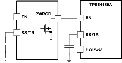 Figure 32. Schematic for Sequential Start-Up Sequence
 Figure 33. Sequential Startup using EN and PWRGD
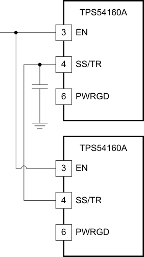 Figure 34. Schematic for Ratiometric Start-Up Using Coupled SS/TR Pins
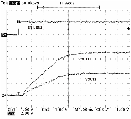 Figure 35. Ratio-Metric Startup using Coupled SS/TR pins
Figure 34 shows a method for ratio-metric start up sequence by connecting the SS/TR pins together. The regulator outputs ramp up to reach regulation at the same time. When calculating the slow start time the pull up current source must be doubled in Equation 6. Figure 35 shows the results of Figure 34.
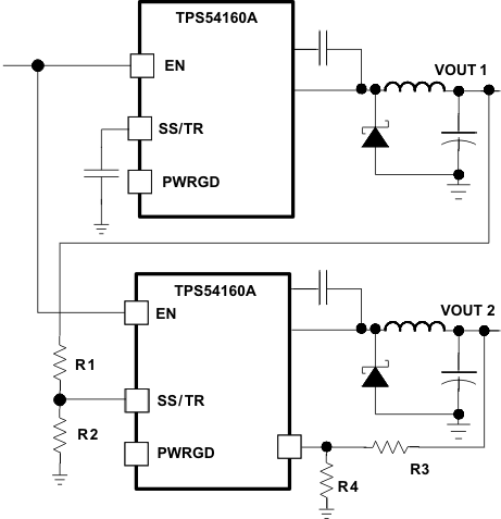 Figure 36. Schematic for Ratiometric and Simultaneous Start-Up Sequence
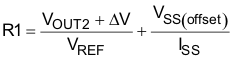
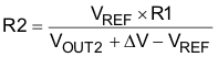
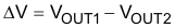
Ratio-metric and simultaneous power supply sequencing can be implemented by connecting the resistor network of R1 and R2 shown in Figure 36 to the output of the power supply that needs to be tracked or another voltage reference source. Using Equation 7 and Equation 8, the tracking resistors can be calculated to initiate the VOUT2 slightly before, after or at the same time as VOUT1. Equation 9 is the voltage difference between VOUT1 and VOUT2 at the 95% of nominal output regulation.
The ΔV variable is zero volts for simultaneous sequencing. To minimize the effect of the inherent SS/TR to VSENSE offset (VSS(offset)) in the slow start circuit and the offset created by the pull-up current source (ISS) and tracking resistors, the VSS(offset) and ISS are included as variables in the equations.
To design a ratio-metric start up in which the VOUT2 voltage is slightly greater than the VOUT1 voltage when VOUT2 reaches regulation, use a negative number in Equation 7 through Equation 9 for ΔV. Equation 9 results in a positive number for applications which the VOUT2 is slightly lower than VOUT1 when VOUT2 regulation is achieved.
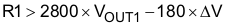
Since the SS/TR pin must be pulled below 40 mV before starting after an EN, UVLO or thermal shutdown fault, careful selection of the tracking resistors is needed to ensure the device restarts after a fault. Make sure the calculated R1 value from Equation 7 is greater than the value calculated in Equation 10 to ensure the device can recover from a fault.
As the SS/TR voltage becomes more than 85% of the nominal reference voltage the VSS(offset) becomes larger as the slow start circuits gradually handoff the regulation reference to the internal voltage reference. The SS/TR pin voltage needs to be greater than 1.3 V for a complete handoff to the internal voltage reference as shown in Figure 23.
8.3.13 Constant Switching Frequency and Timing Resistor (RT/CLK Pin)
The switching frequency of the TPS54160A is adjustable over a wide range from approximately 100kHz to 2500kHz by placing a resistor on the RT/CLK pin. The RT/CLK pin voltage is typically 0.5V and must have a resistor to ground to set the switching frequency. To determine the timing resistance for a given switching frequency, use Equation 11 or the curves in Figure 40 or Figure 41. To reduce the solution size one would typically set the switching frequency as high as possible, but tradeoffs of the supply efficiency, maximum input voltage and minimum controllable on time should be considered.
The minimum controllable on time is typically 130 ns and limits the maximum operating input voltage.
The maximum switching frequency is also limited by the frequency shift circuit. More discussion on the details of the maximum switching frequency is located below.
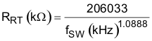
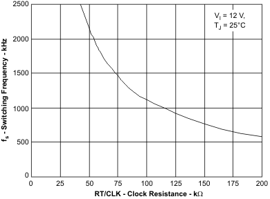 Figure 40. Switching Frequency vs RT/CLK Resistance High Frequency Range
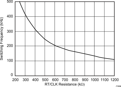 Figure 41. Switching Frequency vs RT/CLK Resistance Low Frequency Range
8.3.14 Overcurrent Protection and Frequency Shift
The TPS54160A implements current mode control which uses the COMP pin voltage to turn off the high-side MOSFET on a cycle by cycle basis. Each cycle the switch current and COMP pin voltage are compared, when the peak switch current intersects the COMP voltage, the high-side switch is turned off. During overcurrent conditions that pull the output voltage low, the error amplifier responds by driving the COMP pin high, increasing the switch current. The error amplifier output is clamped internally, which functions as a switch current limit.
To increase the maximum operating switching frequency at high input voltages the TPS54160A implements a frequency shift. The switching frequency is divided by 8, 4, 2, and 1 as the voltage ramps from 0 to 0.8 volts on VSENSE pin.
The device implements a digital frequency shift to enable synchronizing to an external clock during normal startup and fault conditions. Since the device can only divide the switching frequency by 8, there is a maximum input voltage limit in which the device operates and still have frequency shift protection.
During short-circuit events (particularly with high input voltage applications), the control loop has a finite minimum controllable on time and the output has a low voltage. During the switch on time, the inductor current ramps to the peak current limit because of the high input voltage and minimum on time. During the switch off time, the inductor would normally not have enough off time and output voltage for the inductor to ramp down by the ramp up amount. The frequency shift effectively increases the off time allowing the current to ramp down.
8.3.15 Selecting the Switching Frequency
The switching frequency that is selected should be the lower value of the two equations, Equation 12 and Equation 13. Equation 12 is the maximum switching frequency limitation set by the minimum controllable on time. Setting the switching frequency above this value causes the regulator to skip switching pulses.
Equation 13 is the maximum switching frequency limit set by the frequency shift protection. To have adequate output short circuit protection at high input voltages, the switching frequency should be set to be less than the fSW(maxshift) frequency. In Equation 13, to calculate the maximum switching frequency, consider that the output voltage decreases from the nominal voltage to 0 V, the fDIV integer increases from 1 to 8 corresponding to the frequency shift.
In Figure 42, the solid line illustrates a typical safe operating area regarding frequency shift and assumes the output voltage is 0 V, and the resistance of the inductor is 0.1Ω, FET on-resistance of 0.2 Ω and the diode voltage drop is 0.5 V. The dashed line is the maximum switching frequency to avoid pulse skipping. Enter these equations in a spreadsheet or other software or use the SwitcherPro design software to determine the switching frequency.
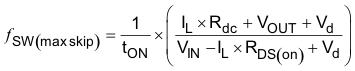
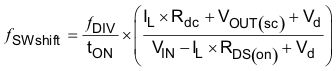
| IL | inductor current |
| Rdc | inductor resistance |
| VIN | maximum input voltage |
| VOUT | output voltage |
| VOUT(sc) | output voltage during short |
| Vd | diode voltage drop |
| RDS(on) | switch on resistance |
| tON | controllable on time |
| ƒDIV | frequency divide equals (1, 2, 4, or 8) |
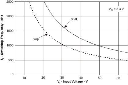 Figure 42. Maximum Switching Frequency vs. Input Voltage
8.3.16 How to Interface to RT/CLK Pin
The RT/CLK pin can be used to synchronize the regulator to an external system clock. To implement the synchronization feature connect a square wave to the RT/CLK pin through the circuit network shown in Figure 43. The square wave amplitude must transition lower than 0.5V and higher than 2.2V on the RT/CLK pin and have an on time greater than 40 ns and an off time greater than 40 ns. The synchronization frequency range is 300 kHz to 2200 kHz. The rising edge of the PH is synchronized to the falling edge of RT/CLK pin signal. The external synchronization circuit should be designed in such a way that the device has the default frequency set resistor connected from the RT/CLK pin to ground should the synchronization signal turn off. It is recommended to use a frequency set resistor connected as shown in Figure 43 through a 50Ω resistor to ground. The resistor should set the switching frequency close to the external CLK frequency. It is recommended to ac couple the synchronization signal through a 10 pF ceramic capacitor to RT/CLK pin and a 4kΩ series resistor. The series resistor reduces PH jitter in heavy load applications when synchronizing to an external clock and in applications which transition from synchronizing to RT mode. The first time the CLK is pulled above the CLK threshold the device switches from the RT resistor frequency to PLL mode. The internal 0.5V voltage source is removed and the CLK pin becomes high impedance as the PLL starts to lock onto the external signal. Since there is a PLL on the regulator the switching frequency can be higher or lower than the frequency set with the external resistor. The device transitions from the resistor mode to the PLL mode and then will increase or decrease the switching frequency until the PLL locks onto the CLK frequency within 100 microseconds.
When the device transitions from the PLL to resistor mode the switching frequency will slow down from the CLK frequency to 150 kHz, then reapply the 0.5V voltage and the resistor will then set the switching frequency. The switching frequency is divided by 8, 4, 2, and 1 as the voltage ramps from 0 to 0.8 volts on VSENSE pin. The device implements a digital frequency shift to enable synchronizing to an external clock during normal startup and fault conditions. Figure 44, Figure 45 and Figure 46 show the device synchronized to an external system clock in continuous conduction mode (ccm) discontinuous conduction (dcm) and pulse skip mode (psm).
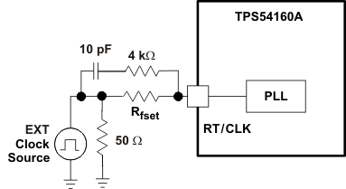 Figure 43. Synchronizing to a System Clock
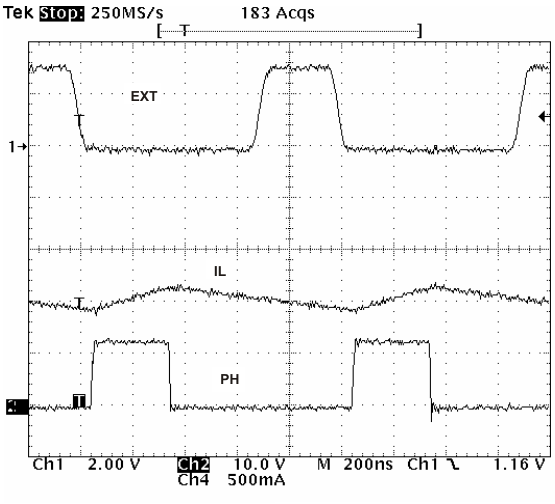 Figure 44. Plot of Synchronizing in CCM
 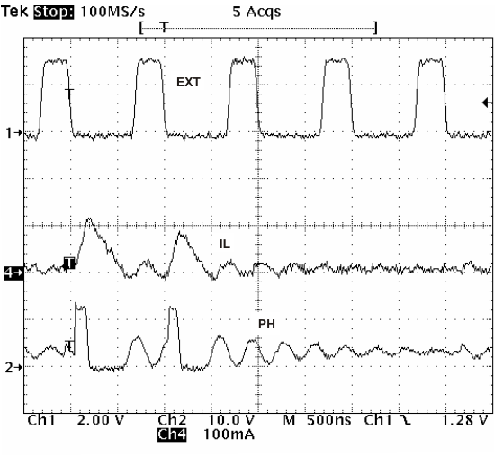 Figure 46. Plot of Synchronizing in PSM
 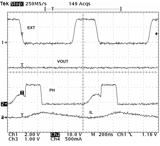 Figure 45. Plot of Synchronizing in DCM
 8.3.17 Power Good (PWRGD Pin)
The PWRGD pin is an open drain output. Once the VSENSE pin is between 94% and 107% of the internal voltage reference the PWRGD pin is de-asserted and the pin floats. It is recommended to use a pull-up resistor between the values of 10 and 100kΩ to a voltage source that is 5.5V or less. The PWRGD is in a defined state once the VIN input voltage is greater than 1.5V but with reduced current sinking capability. The PWRGD will achieve full current sinking capability as VIN input voltage approaches 3V.
The PWRGD pin is pulled low when the VSENSE is lower than 92% or greater than 109% of the nominal internal reference voltage. Also, the PWRGD is pulled low, if the UVLO or thermal shutdown are asserted or the EN pin pulled low.
8.3.18 Overvoltage Transient Protection
The TPS54160A incorporates an overvoltage transient protection (OVTP) circuit to minimize voltage overshoot when recovering from output fault conditions or strong unload transients on power supply designs with low value output capacitance. For example, when the power supply output is overloaded the error amplifier compares the actual output voltage to the internal reference voltage. If the VSENSE pin voltage is lower than the internal reference voltage for a considerable time, the output of the error amplifier will respond by clamping the error amplifier output to a high voltage. Thus, requesting the maximum output current. Once the condition is removed, the regulator output rises and the error amplifier output transitions to the steady state duty cycle. In some applications, the power supply output voltage can respond faster than the error amplifier output can respond, this actuality leads to the possibility of an output overshoot. The OVTP feature minimizes the output overshoot, when using a low value output capacitor, by implementing a circuit to compare the VSENSE pin voltage to OVTP threshold which is 109% of the internal voltage reference. If the VSENSE pin voltage is greater than the OVTP threshold, the high-side MOSFET is disabled preventing current from flowing to the output and minimizing output overshoot. When the VSENSE voltage drops lower than the OVTP threshold, the high-side MOSFET is allowed to turn on at the next clock cycle.
8.3.19 Thermal Shutdown
The device implements an internal thermal shutdown to protect itself if the junction temperature exceeds 182°C. The thermal shutdown forces the device to stop switching when the junction temperature exceeds the thermal trip threshold. Once the die temperature decreases below 182°C, the device reinitiates the power up sequence by discharging the SS/TR pin.
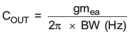
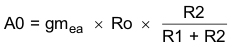
8.3.20 Small Signal Model for Loop Response
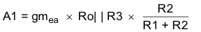
Figure 47 shows an equivalent model for the TPS54160A control loop which can be modeled in a circuit simulation program to check frequency response and dynamic load response. The error amplifier is a transconductance amplifier with a gmEA of 97 μA/V. The error amplifier can be modeled using an ideal voltage controlled current source. The resistor RO and capacitor CO model the open loop gain and frequency response of the amplifier. The 1mV ac voltage source between the nodes a and b effectively breaks the control loop for the frequency response measurements. Plotting c/a shows the small signal response of the frequency compensation. Plotting a/b shows the small signal response of the overall loop. The dynamic loop response can be checked by replacing RL with a current source with the appropriate load step amplitude and step rate in a time domain analysis. This equivalent model is only valid for continuous conduction mode designs.
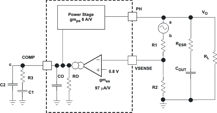 Figure 47. Small Signal Model for Loop Response
8.3.21 Simple Small Signal Model for Peak Current Mode Control
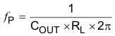
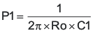
Figure 48 describes a simple small signal model that can be used to understand how to design the frequency compensation. The TPS54160A power stage can be approximated to a voltage-controlled current source (duty cycle modulator) supplying current to the output capacitor and load resistor. The control to output transfer function is shown in Equation 14 and consists of a dc gain, one dominant pole, and one ESR zero. The quotient of the change in switch current and the change in COMP pin voltage (node c in Figure 47) is the power stage transconductance. The gmPS for the TPS54160A is 6 A/V. The low-frequency gain of the power stage frequency response is the product of the transconductance and the load resistance as shown in Equation 15.
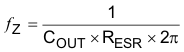
As the load current increases and decreases, the low-frequency gain decreases and increases, respectively. This variation with the load may seem problematic at first glance, but fortunately the dominant pole moves with the load current (see Equation 16). The combined effect is highlighted by the dashed line in the right half of Figure 48. As the load current decreases, the gain increases and the pole frequency lowers, keeping the 0-dB crossover frequency the same for the varying load conditions which makes it easier to design the frequency compensation. The type of output capacitor chosen determines whether the ESR zero has a profound effect on the frequency compensation design. Using high ESR aluminum electrolytic capacitors may reduce the number frequency compensation components needed to stabilize the overall loop because the phase margin increases from the ESR zero at the lower frequencies (see Equation 17).
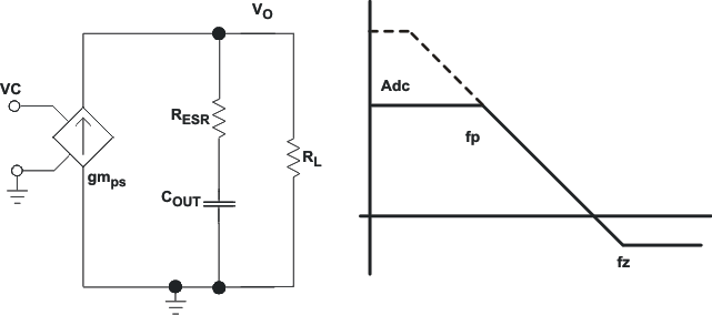 Figure 48. Simple Small Signal Model and Frequency Response for Peak Current Mode Control
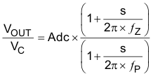

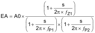
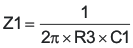
8.3.22 Small Signal Model for Frequency Compensation
The TPS54160A uses a transconductance amplifier for the error amplifier and readily supports three of the commonly-used frequency compensation circuits. Compensation circuits Type 2A, Type 2B, and Type 1 are shown in Figure 49. Type 2 circuits most likely implemented in high bandwidth power-supply designs using low ESR output capacitors. The Type 1 circuit is used with power-supply designs with high-ESR aluminum electrolytic or tantalum capacitors.. Equation 18 and Equation 19 show how to relate the frequency response of the amplifier to the small signal model in Figure 49. The open-loop gain and bandwidth are modeled using the RO and CO shown in Figure 49. See the application section for a design example using a Type 2A network with a low ESR output capacitor.
Equation 18 through Equation 27 are provided as a reference for those who prefer to compensate using the preferred methods. Those who prefer to use prescribed method use the method outlined in the application section or use switched information.
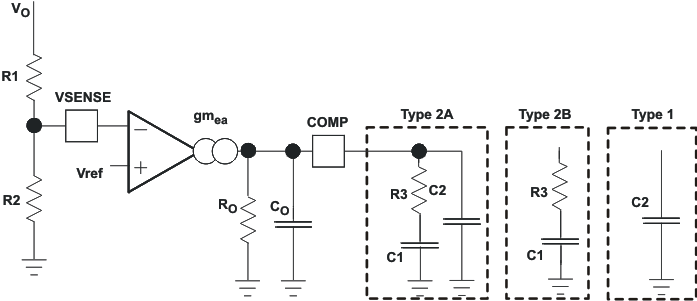 Figure 49. Types of Frequency Compensation
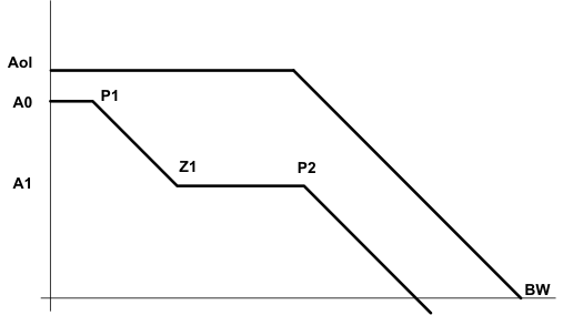 Figure 50. Frequency Response of the Type 2A and Type 2B Frequency Compensation
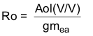


8.4 Device Functional Modes
8.4.1 Operation with VIN < 3.5 V (Minimum VIN)
The device is recommended to operate with input voltages above 3.5 V. The typical VIN UVLO threshold is 2.5 V and the device may operate at input voltages down to the UVLO voltage. At input voltages below the actual UVLO voltage, the device will not switch. The PWRGD output will be controlled once VIN is above 1.5 V maximum. If EN is externally pulled up to VIN or left floating, when VIN passes the UVLO threshold the device will become active. Switching is enabled the soft start sequence is initiated. The TPS54160 will start at the soft start time determined by the external soft start capacitor at the SS/TR pin.
8.4.2 Operation with EN Control
The enable threshold voltage is 1.25 V typical. With EN held below that voltage the device is disabled and switching is inhibited even if VIN is above its UVLO threshold. The IC quiescent current is reduced in this state. If the EN voltage is increased above the threshold while VIN is above its UVLO threshold, the device becomes active. Switching is enabled, and the soft start sequence is initiated. The TPS54160 will start at the soft start time determined by the external slow start capacitor at the SS/TR pin.