SLUSCO8B November   2016  – June 2018 TPS54200 , TPS54201

PRODUCTION DATA.  

  1. Features
  2. Applications
  3. Description
    1.     Device Images
      1.      Simplified Schematic
      2.      Excellent Deep Dimming in ADIM
  4. Revision History
  5. Description (continued)
  6. Pin Configuration and Functions
    1.     Pin Functions
  7. Specifications
    1. 7.1 Absolute Maximum Ratings
    2. 7.2 ESD Ratings
    3. 7.3 Recommended Operating Conditions
    4. 7.4 Thermal Information
    5. 7.5 Electrical Characteristics
    6. 7.6 Timing Requirements
    7. 7.7 Switching Characteristics
    8. 7.8 Typical Characteristics
  8. Detailed Description
    1. 8.1 Overview
    2. 8.2 Functional Block Diagram
    3. 8.3 Feature Description
      1. 8.3.1  Fixed-Frequency PWM Control
      2. 8.3.2  Error Amplifier
      3. 8.3.3  Slope Compensation and Output Current
      4. 8.3.4  Input Undervoltage Lockout
      5. 8.3.5  Voltage Reference
      6. 8.3.6  Setting LED Current
      7. 8.3.7  Internal Soft Start
      8. 8.3.8  Bootstrap Voltage (BOOT)
      9. 8.3.9  Overcurrent Protection
        1. 8.3.9.1 High-Side MOSFET Overcurrent Protection
        2. 8.3.9.2 Low-Side MOSFET Overcurrent Protection
        3. 8.3.9.3 Low-Side MOSFET Reverse Overcurrent Protection
      10. 8.3.10 Fault Protection
        1. 8.3.10.1 LED-Open Protection
        2. 8.3.10.2 LED Short Protection
        3. 8.3.10.3 Sense-Resistor Short Protection
        4. 8.3.10.4 Sense-Resistor Open Protection
        5. 8.3.10.5 Overvoltage Protection
        6. 8.3.10.6 Thermal Shutdown
    4. 8.4 Device Functional Modes
      1. 8.4.1 Enable and Disable Device
      2. 8.4.2 Mode Detection
      3. 8.4.3 Analog Dimming Mode Operation
      4. 8.4.4 PWM Dimming-Mode Operation
  9. Application and Implementation
    1. 9.1 Application Information
    2. 9.2 Typical Application
      1. 9.2.1 TPS5420x 12-V Input, 1.5-A, 3-Piece IR LED Driver With Analog Dimming
        1. 9.2.1.1 Design Requirements
        2. 9.2.1.2 Detailed Design Procedure
          1. 9.2.1.2.1 Inductor Selection
          2. 9.2.1.2.2 Input Capacitor Selection
          3. 9.2.1.2.3 Output Capacitor Selection
          4. 9.2.1.2.4 FB Pin RC Filter Selection
          5. 9.2.1.2.5 Sense Resistor Selection
        3. 9.2.1.3 Application Curves
      2. 9.2.2 TPS5420x 24-V Input, 1-A, 4-Piece WLED Driver With PWM Dimming
        1. 9.2.2.1 Design Requirements
        2. 9.2.2.2 Detailed Design Procedure
          1. 9.2.2.2.1 Inductor Selection
          2. 9.2.2.2.2 Input Capacitor Selection
          3. 9.2.2.2.3 Output Capacitor Selection
          4. 9.2.2.2.4 FB Pin RC Filter Selection
          5. 9.2.2.2.5 Sense Resistor Selection
        3. 9.2.2.3 Application Curves
  10. 10Power Supply Recommendations
  11. 11Layout
    1. 11.1 Layout Guidelines
    2. 11.2 Layout Example
  12. 12Device and Documentation Support
    1. 12.1 Device Support
      1. 12.1.1 Third-Party Products Disclaimer
    2. 12.2 Documentation Support
      1. 12.2.1 Related Links
    3. 12.3 Receiving Notification of Documentation Updates
    4. 12.4 Community Resources
    5. 12.5 Trademarks
    6. 12.6 Electrostatic Discharge Caution
    7. 12.7 Glossary
  13. 13Mechanical, Packaging, and Orderable Information

Package Options

Mechanical Data (Package|Pins)
Thermal pad, mechanical data (Package|Pins)
Orderable Information

Application Curves

TPS54200 TPS54201 fig37_lusco8.gif
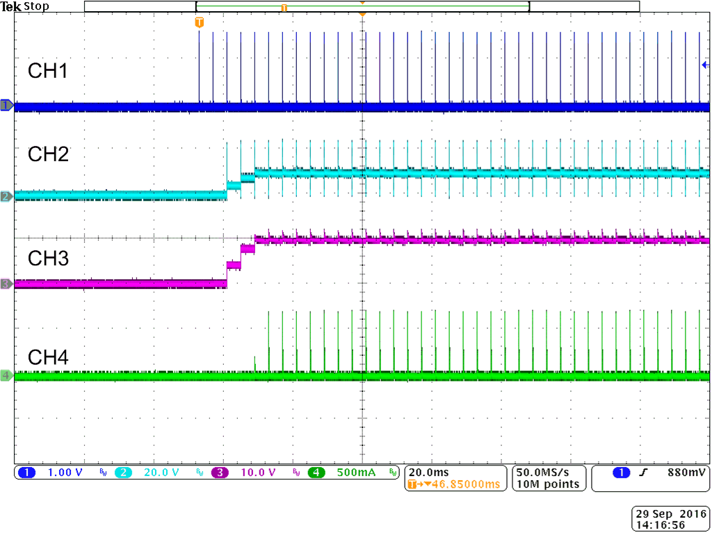
CH1: PWM CH2: SW CH3: VOUT CH4: LED current
Figure 41. Start-Up at 1% PWM Duty Cycle and 250 Hz
TPS54200 TPS54201 fig39_lusco8.gif
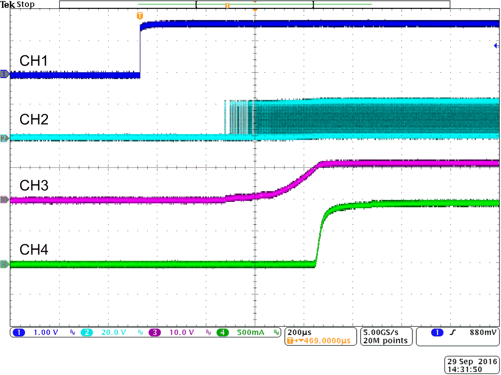
CH1: PWM CH2: SW CH3: VOUT CH4: LED Current
Figure 43. Start-Up at 100% PWM Duty Cycle
TPS54200 TPS54201 fig41_lusco8.gif
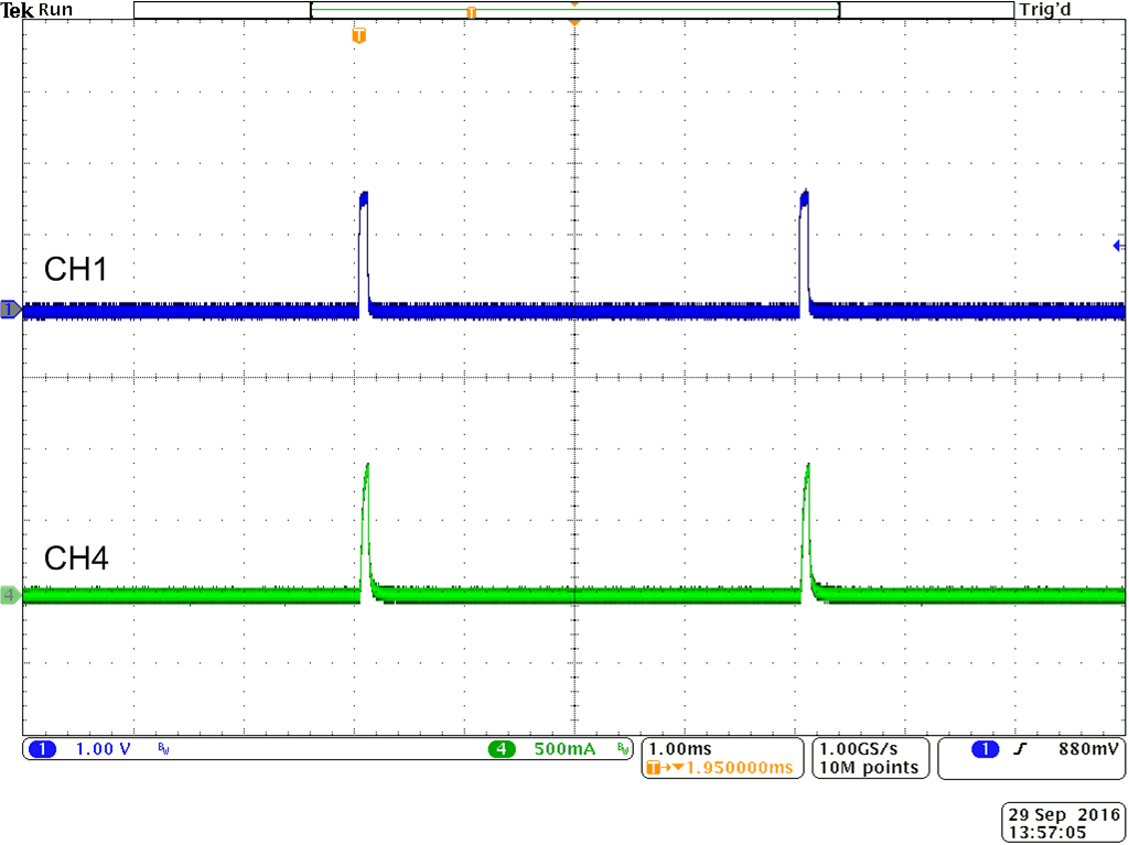
CH1 PWM CH4: LED current
Figure 45. PWM Dimming With 2% Duty Cycle and 250 Hz
TPS54200 TPS54201 fig43_lusco8.gif
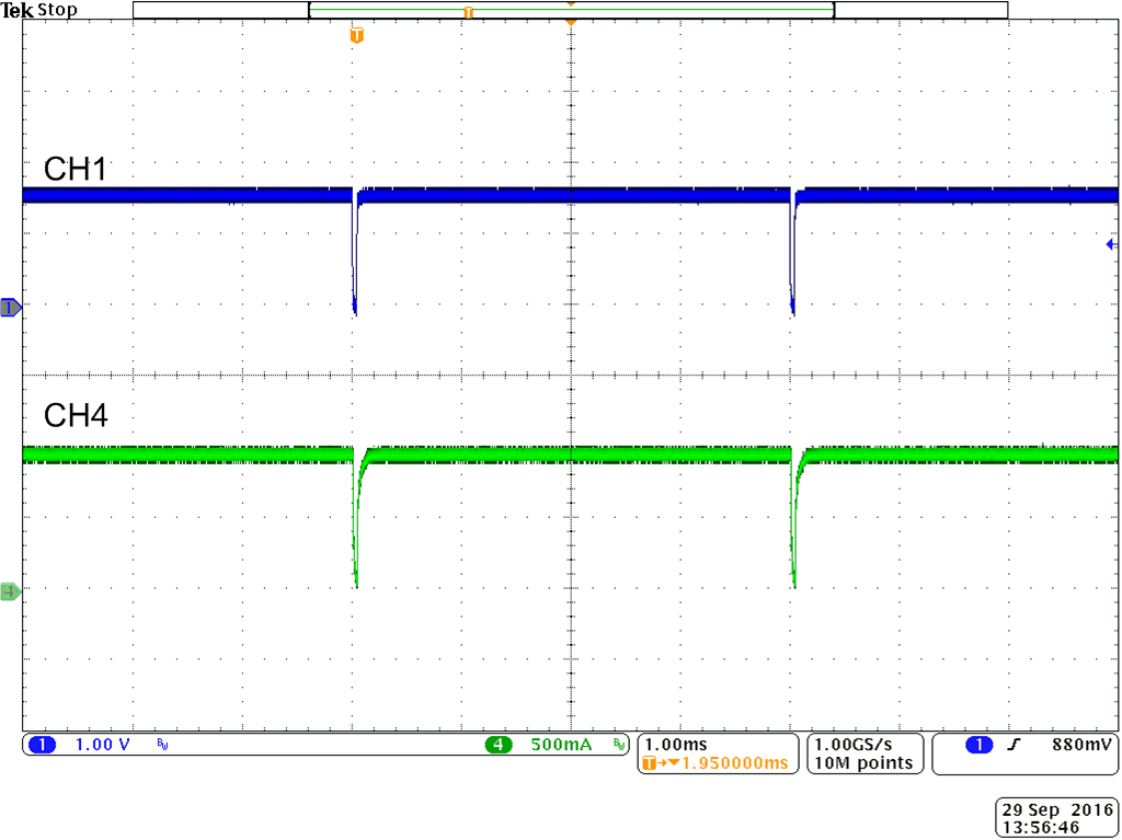
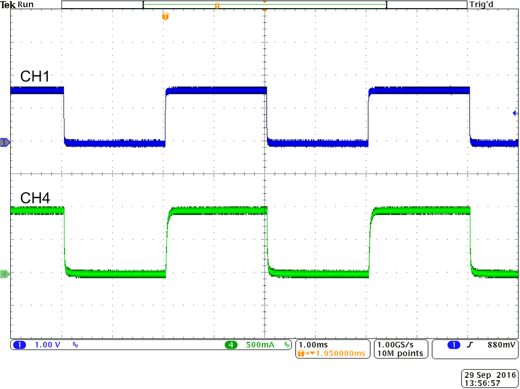
CH1: PWM CH4: LED current
Figure 47. PWM Dimming With 99% Duty Cycle and 250 Hz
TPS54200 TPS54201 fig45_lusco8.gif
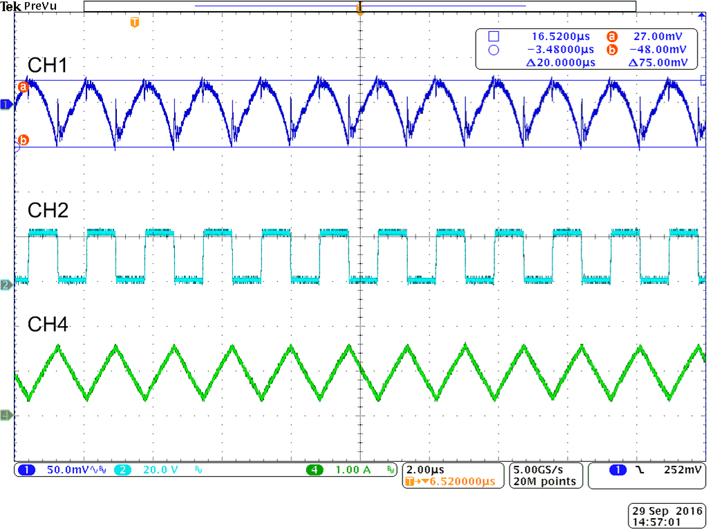
CH1: VVIN CH2: SW CH4: Inductor current
(AC-coupled)
Figure 49. Input Voltage Ripple at 100% PWM Duty Cycle
TPS54200 TPS54201 fig38_lusco8.gif
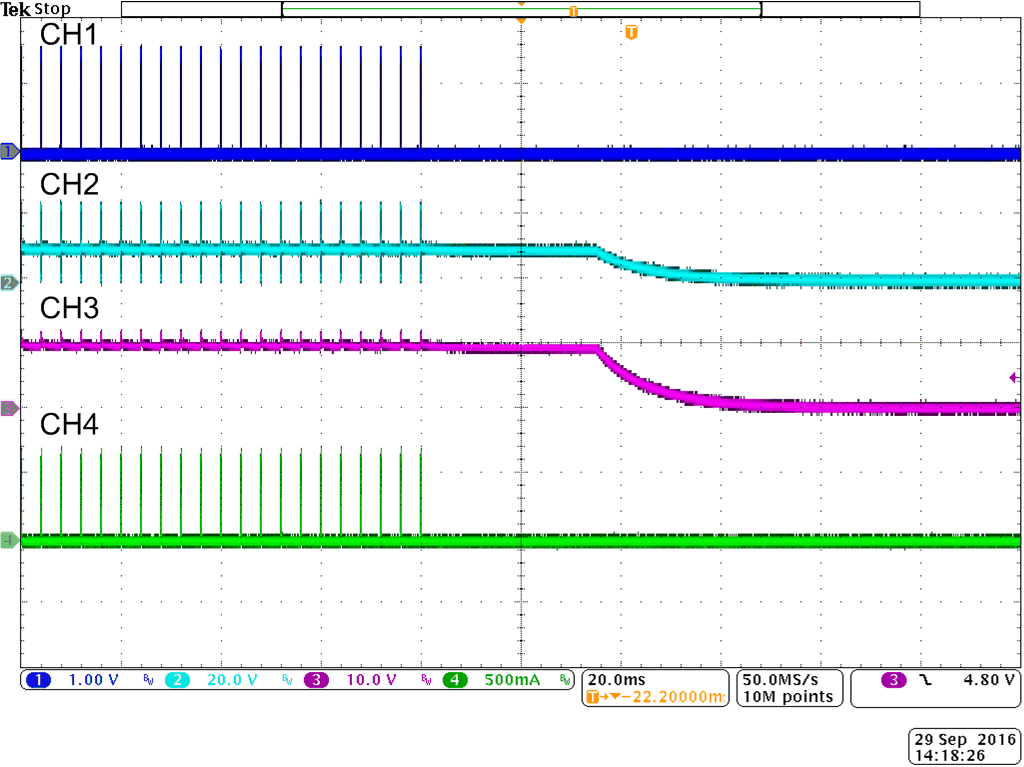
CH1: PWM CH2: SW CH3: VOUT CH4: LED current
Figure 42. Shutdown at 1% PWM Duty Cycle and 250 Hz
TPS54200 TPS54201 fig40_lusco8.gif
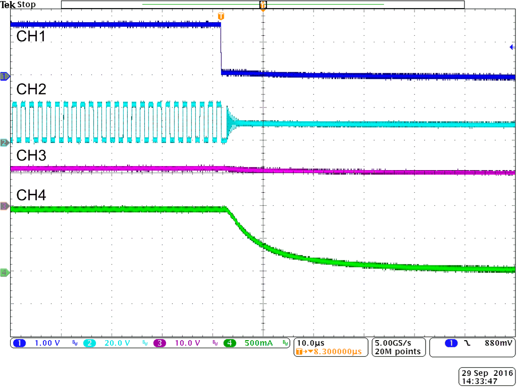
CH1: PWM CH2: SW CH3: VOUT CH4: LED current
Figure 44. Shutdown at 100% PWM Duty Cycle
TPS54200 TPS54201 fig42_lusco8.gif
CH1: PWM CH4: LED current
Figure 46. PWM Dimming With 50% Duty Cycle and 250 Hz
TPS54200 TPS54201 fig44_lusco8.gif
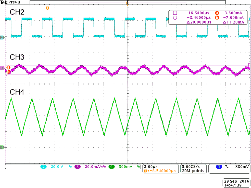
CH2: SW CH3: LED current CH4: Inductor current
(AC-coupled)
Figure 48. LED Current Ripple at 100% PWM Duty Cycle