SLUS851D October 2008 – October 2014 TPS54231
PRODUCTION DATA.
- 1 Features
- 2 Applications
- 3 Description
- 4 Simplified Schematic
- 5 Revision History
- 6 Pin Configuration and Functions
- 7 Specifications
-
8 Detailed Description
- 8.1 Overview
- 8.2 Functional Block Diagram
- 8.3
Feature Description
- 8.3.1 Fixed-Frequency PWM Control
- 8.3.2 Voltage Reference (Vref)
- 8.3.3 Bootstrap Voltage (BOOT)
- 8.3.4 Enable and Adjustable Input Undervoltage Lockout (VIN UVLO)
- 8.3.5 Programmable Slow Start Using SS Pin
- 8.3.6 Error Amplifier
- 8.3.7 Slope Compensation
- 8.3.8 Current-Mode Compensation Design
- 8.3.9 Overcurrent Protection and Frequency Shift
- 8.3.10 Overvoltage Transient Protection
- 8.3.11 Thermal Shutdown
- 8.4 Device Functional Modes
-
9 Application and Implementation
- 9.1 Application Information
- 9.2
Typical Application
- 9.2.1 Design Requirements
- 9.2.2 Detailed Design Procedure
- 9.2.3 Application Curves
- 10Power Supply Recommendations
- 11Layout
- 12Device and Documentation Support
- 13Mechanical, Packaging, and Orderable Information
Package Options
Mechanical Data (Package|Pins)
- D|8
Thermal pad, mechanical data (Package|Pins)
Orderable Information
6 Pin Configuration and Functions
D Package
8-Pin SOIC
Top View
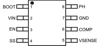
Pin Functions
| PIN | I/O | DESCRIPTION | |
|---|---|---|---|
| NO. | NAME | ||
| 1 | BOOT | O | A 0.1-μF bootstrap capacitor is required between the BOOT and PH pins. If the voltage on this capacitor falls below the minimum requirement, the high-side MOSFET is forced to switch off until the capacitor is refreshed. |
| 2 | VIN | I | This pin is the 3.5- to 28-V input supply voltage. |
| 3 | EN | I | This pin is the enable pin. To disable, pull below 1.25 V. Float this pin to enable. Programming the input undervoltage lockout with two resistors is recommended. |
| 4 | SS | I | This pin is slow-start pin. An external capacitor connected to this pin sets the output rise time. |
| 5 | VSENSE | I | This pin is the inverting node of the transconductance (gm) error amplifier. |
| 6 | COMP | O | This pin is the error-amplifier output and input to the PWM comparator. Connect frequency compensation components to this pin. |
| 7 | GND | — | Ground pin |
| 8 | PH | O | The PH pin is the source of the internal high-side power MOSFET. |