SLVSA86D March 2010 – October 2018 TPS54260
PRODUCTION DATA.
- 1 Features
- 2 Applications
- 3 Description
- 4 Revision History
- 5 Pin Configuration and Functions
- 6 Specifications
-
7 Detailed Description
- 7.1 Overview
- 7.2 Functional Block Diagram
- 7.3
Feature Description
- 7.3.1 Fixed Frequency PWM Control
- 7.3.2 Slope Compensation Output Current
- 7.3.3 Pulse-Skip Eco-Mode
- 7.3.4 Low-Dropout Operation and Bootstrap Voltage (BOOT)
- 7.3.5 Error Amplifier
- 7.3.6 Voltage Reference
- 7.3.7 Adjusting the Output Voltage
- 7.3.8 Enable and Adjusting Undervoltage Lockout
- 7.3.9 Slow-Start / Tracking Pin (SS/TR)
- 7.3.10 Overload Recovery Circuit
- 7.3.11 Sequencing
- 7.3.12 Constant Switching Frequency and Timing Resistor (RT/CLK Pin)
- 7.3.13 Overcurrent Protection and Frequency Shift
- 7.3.14 Selecting the Switching Frequency
- 7.3.15 How to Interface to RT/CLK Pin
- 7.3.16 Powergood (PWRGD Pin)
- 7.3.17 Overvoltage Transient Protection
- 7.3.18 Thermal Shutdown
- 7.3.19 Small Signal Model for Loop Response
- 7.3.20 Simple Small Signal Model for Peak Current Mode Control
- 7.3.21 Small Signal Model for Frequency Compensation
- 7.4 Device Functional Modes
-
8 Application and Implementation
- 8.1 Application Information
- 8.2
Typical Applications
- 8.2.1
3.3-V Output Application
- 8.2.1.1 Design Requirements
- 8.2.1.2
Detailed Design Procedure
- 8.2.1.2.1 Custom Design With WEBENCH® Tools
- 8.2.1.2.2 Selecting the Switching Frequency
- 8.2.1.2.3 Output Inductor Selection (LO)
- 8.2.1.2.4 Output Capacitor
- 8.2.1.2.5 Catch Diode
- 8.2.1.2.6 Input Capacitor
- 8.2.1.2.7 Slow-Start Capacitor
- 8.2.1.2.8 Bootstrap Capacitor Selection
- 8.2.1.2.9 Undervoltage Lock Out Set Point
- 8.2.1.2.10 Output Voltage and Feedback Resistors Selection
- 8.2.1.2.11 Compensation
- 8.2.1.2.12 Discontinuous Mode and Eco-Mode Boundary
- 8.2.1.2.13 Power Dissipation Estimate
- 8.2.1.3 Application Curves
- 8.2.2 Inverting Power Supply
- 8.2.3 Split-Rail Power Supply
- 8.2.4 12-V to 3.8-V GSM Power Supply
- 8.2.5 24-V to 4.2-V GSM Power Supply
- 8.2.1
3.3-V Output Application
- 9 Power Supply Recommendations
- 10Layout
- 11Device and Documentation Support
- 12Mechanical, Packaging, and Orderable Information
Package Options
Mechanical Data (Package|Pins)
Thermal pad, mechanical data (Package|Pins)
Orderable Information
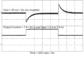
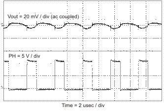
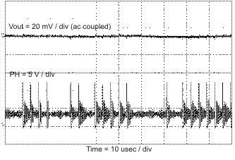
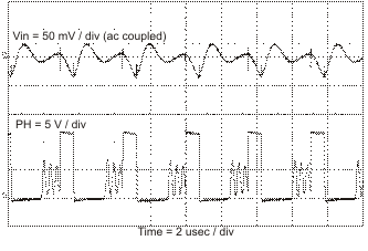
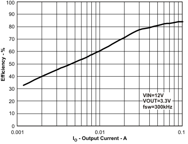
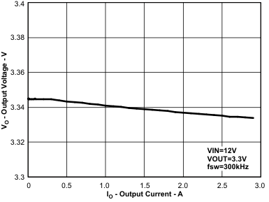
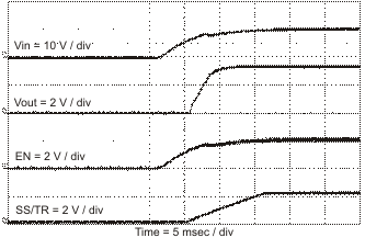
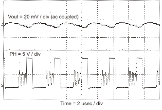
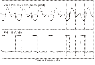
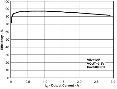
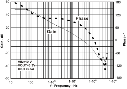
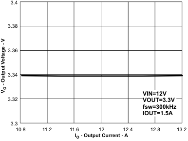
8.2.1.3 Application Curves
