SLVS632K January 2006 – January 2024 TPS5430 , TPS5431
PRODUCTION DATA
- 1
- 1 Features
- 2 Applications
- 3 Description
- 4 Pin Configuration and Functions
- 5 Specifications
-
6 Detailed Description
- 6.1 Overview
- 6.2 Functional Block Diagram
- 6.3
Feature Description
- 6.3.1 Oscillator Frequency
- 6.3.2 Voltage Reference
- 6.3.3 Enable (ENA) and Internal Slow Start
- 6.3.4 Undervoltage Lockout (UVLO)
- 6.3.5 Boost Capacitor (BOOT)
- 6.3.6 Output Feedback (VSENSE) and Internal Compensation
- 6.3.7 Voltage Feed-Forward
- 6.3.8 Pulse-Width-Modulation (PWM) Control
- 6.3.9 Overcurrent Limiting
- 6.3.10 Overvoltage Protection
- 6.3.11 Thermal Shutdown
- 6.4 Device Functional Modes
-
7 Application and Implementation
- 7.1 Application Information
- 7.2
Typical Applications
- 7.2.1
12-V Input to 5.0-V Output
- 7.2.1.1 Design Requirements
- 7.2.1.2 Detailed Design Procedure
- 7.2.1.3 Application Curves
- 7.2.2 Wide Input Voltage Ranges with TPS5430
- 7.2.3 Circuit Using Ceramic Output Filter Capacitors
- 7.2.1
12-V Input to 5.0-V Output
- 7.3 Power Supply Recommendations
- 7.4 Layout
- 8 Device and Documentation Support
- 9 Revision History
- 10Mechanical, Packaging, and Orderable Information
Package Options
Refer to the PDF data sheet for device specific package drawings
Mechanical Data (Package|Pins)
- DDA|8
Thermal pad, mechanical data (Package|Pins)
Orderable Information
7.2.1.2.4.1 Inductor Selection
To calculate the minimum value of the output inductor, use Equation 4:
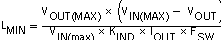
KIND is a coefficient that represents the amount of inductor ripple current relative to the maximum output current. Three things need to be considered when determining the amount of ripple current in the inductor: the peak to peak ripple current affects the output ripple voltage amplitude, the ripple current affects the peak switch current and the amount of ripple current determines at what point the circuit becomes discontinuous. For designs using the TPS5430, KIND of 0.2 to 0.3 yields good results. Low output ripple voltages can be obtained when paired with the proper output capacitor, the peak switch current will be well below the current limit set point and relatively low load currents can be sourced before discontinuous operation.
For this design example use KIND = 0.2 and the minimum inductor value is calculated to be 12.5 μH. The next highest standard value is 15 μH, which is used in this design.
For the output filter inductor it is important that the RMS current and saturation current ratings not be exceeded. The RMS inductor current can be found from Equation 5:
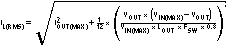
and the peak inductor current can be determined with Equation 6:
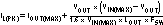
For this design, the RMS inductor current is 3.003 A, and the peak inductor current is 3.31 A. The chosen inductor is a Sumida CDRH104R-150 15 μH. It has a saturation current rating of 3.4 A and a RMS current rating of 3.6 A, easily meeting these requirements. A lesser rated inductor can be used, however this device was chosen because of its low profile component height. In general, inductor values for use with the TPS5430 are in the range of 10 μH to 100 μH.