SLUSCV2A June 2017 – April 2021 TPS54308
PRODUCTION DATA
- 1 Features
- 2 Applications
- 3 Description
- 4 Revision History
- 5 Pin Configuration and Functions
- 6 Specifications
-
7 Detailed Description
- 7.1 Overview
- 7.2 Functional Block Diagram
- 7.3
Feature Description
- 7.3.1 Fixed-Frequency PWM Control
- 7.3.2 Force Continuous Conduction Mode (FCCM)
- 7.3.3 Error Amplifier
- 7.3.4 Slope Compensation and Output Current
- 7.3.5 Enable and Adjusting Undervoltage Lockout
- 7.3.6 Safe Start-Up into Pre-Biased Outputs
- 7.3.7 Voltage Reference
- 7.3.8 Adjusting Output Voltage
- 7.3.9 Internal Soft Start
- 7.3.10 Bootstrap Voltage (BOOT)
- 7.3.11 Overcurrent Protection
- 7.3.12 Output Overvoltage Protection (OVP)
- 7.3.13 Thermal Shutdown
- 7.4 Device Functional Modes
-
8 Application and Implementation
- 8.1 Application Information
- 8.2
Typical Application
- 8.2.1 TPS54308 8-V to 28-V Input, 5-V Output Converter
- 8.2.2 Design Requirements
- 8.2.3 Detailed Design Procedure
- 8.2.4 Application Curves
- 9 Power Supply Recommendations
- 10Layout
- 11Device and Documentation Support
- 12Mechanical, Packaging, and Orderable Information
Package Options
Mechanical Data (Package|Pins)
- DDC|6
Thermal pad, mechanical data (Package|Pins)
Orderable Information
3 Description
The TPS54308 is a 4.5-V to 28-V input voltage range, 3-A synchronous buck converter. The device includes two integrated switching FETs, internal loop compensation, and 5-ms internal soft start to reduce component count.
By integrating the MOSFETs and employing the SOT-23 package, the TPS54308 achieves high power density and offers a small footprint on the PCB.
The TPS54308 operates in force continuous conduction mode (FCCM) during light load conditions. The switching frequency is maintained at an almost constant level over entire load range.
Cycle-by-cycle current limit in both high-side MOSFETs protects the converter in an overload condition and is enhanced by a low-side MOSFET freewheeling current limit, which prevents current runaway. Hiccup mode protection is triggered if the overcurrent condition has persisted for longer than the present time.
| PART NUMBER | PACKAGE(1) | BODY SIZE (NOM) |
|---|---|---|
| TPS54308 | SOT-23(6) | 1.60 mm × 2.90 mm |
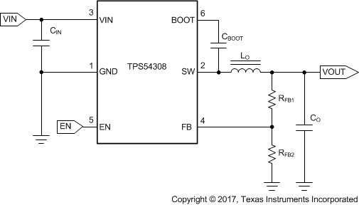
 Simplified Schematic
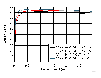
 Efficiency Versus Output
Current