SLVS932F May 2009 – November 2014 TPS54325
PRODUCTION DATA.
- 1 Features
- 2 Applications
- 3 Description
- 4 Simplified Schematic
- 5 Revision History
- 6 Pin Configuration and Functions
- 7 Specifications
- 8 Detailed Description
- 9 Application and Implementation
- 10Power Supply Recommendations
- 11Layout
- 12Device and Documentation Support
- 13Mechanical, Packaging, and Orderable Information
Package Options
Mechanical Data (Package|Pins)
- PWP|14
Thermal pad, mechanical data (Package|Pins)
- PWP|14
Orderable Information
7 Specifications
7.1 Absolute Maximum Ratings
over operating free-air temperature range (unless otherwise noted)(1)| MIN | MAX | UNIT | |||
|---|---|---|---|---|---|
| VI | Input voltage range | VIN, VCC, EN | –0.3 | 20 | V |
| VBST | –0.3 | 26 | V | ||
| VBST (vs SW1, SW2) | –0.3 | 6.5 | V | ||
| VFB, VO, SS, PG | –0.3 | 6.5 | V | ||
| SW1, SW2 | –2 | 20 | V | ||
| SW1, SW2 (10 ns transient) | –3 | 20 | V | ||
| VO | Output voltage range | VREG5 | –0.3 | 6.5 | V |
| PGND1, PGND2 | –0.3 | 0.3 | V | ||
| Vdiff | Voltage from GND to POWERPAD | –0.2 | 0.2 | V | |
| TJ | Operating junction temperature | –40 | 150 | °C | |
(1) Stresses beyond those listed under absolute maximum ratings may cause permanent damage to the device. These are stress ratings only, and functional operation of the device at these or any other conditions beyond those indicated under recommended operating conditions is not implied. Exposure to absolute-maximum-rated conditions for extended periods may affect device reliability.
7.2 Handling Ratings
| MIN | MAX | UNIT | |||
|---|---|---|---|---|---|
| Tstg | Storage temperature range | –55 | 150 | °C | |
| V(ESD) | Electrostatic discharge | Human body model (HBM), per ANSI/ESDA/JEDEC JS-001, all pins(1) | 2000 | V | |
| Charged device model (CDM), per JEDEC specification JESD22-C101, all pins(2) | 500 | ||||
(1) JEDEC document JEP155 states that 2000-V HBM allows safe manufacturing with a standard ESD control process.
(2) JEDEC document JEP157 states that 500-V CDM allows safe manufacturing with a standard ESD control process.
7.3 Thermal Information
| THERMAL METRIC(1) | PWP | UNIT | |
|---|---|---|---|
| 12 PINS | |||
| RθJA | Junction-to-ambient thermal resistance | 55.6 | °C/W |
| RθJC(top) | Junction-to-case (top) thermal resistance | 51.3 | |
| RθJB | Junction-to-board thermal resistance | 26.4 | |
| ψJT | Junction-to-top characterization parameter | 1.8 | |
| ψJB | Junction-to-board characterization parameter | 20.6 | |
| RθJC(bot) | Junction-to-case (bottom) thermal resistance | 4.3 | |
(1) For more information about traditional and new thermal metrics, see the IC Package Thermal Metrics application report, SPRA953.
7.4 Recommended Operating Conditions
over operating free-air temperature range (unless otherwise noted)| MIN | MAX | UNIT | |||
|---|---|---|---|---|---|
| VCC | Supply input voltage range | 4.5 | 18 | V | |
| VIN | Power input voltage range | 2 | 18 | V | |
| VI | Input voltage range | VBST | –0.1 | 24 | V |
| VBST (vs SW1, SW2) | –0.1 | 6 | |||
| SS, PG | –0.1 | 6 | |||
| EN | –0.1 | 18 | |||
| VO, VFB | –0.1 | 5.5 | |||
| SW1, SW2 | –1.8 | 18 | |||
| SW1, SW2 (10 ns transient) | –3 | 18 | |||
| PGND1, PGND2 | –0.1 | 0.1 | |||
| VO | Output voltage range | VREG5 | –0.1 | 6 | V |
| IO | Output current range | IVREG5 | 0 | 10 | mA |
| TA | Operating free-air temperature | –40 | 85 | °C | |
| TJ | Operating junction temperature | –40 | 125 | °C | |
7.5 Electrical Characteristics
over operating free-air temperature range, VCC, VIN = 12 V (unless otherwise noted)| PARAMETER | TEST CONDITIONS | MIN | TYP | MAX | UNIT | |
|---|---|---|---|---|---|---|
| SUPPLY CURRENT | ||||||
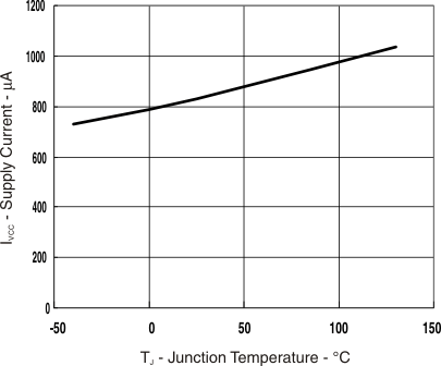
| IVCC | Operating - non-switching supply current | VCC current, TA = 25°C, EN = 5 V, VFB = 0.8 V |
850 | 1300 | μA | |
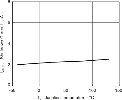
| IVCCSDN | Shutdown supply current | VCC current, TA = 25°C, EN = 0 V | 10 | μA | ||
| LOGIC THRESHOLD | ||||||
| VENH | EN high-level input voltage | EN | 1.6 | V | ||
| VENL | EN low-level input voltage | EN | 0.4 | V | ||
| VFB VOLTAGE AND DISCHARGE RESISTANCE | ||||||
| VFBTH | VFB threshold voltage | TA = 25°C, VO = 1.05 V | 757 | 765 | 773 | mV |
| TA = 0°C to 85°C, VO = 1.05 V(1) | 753 | 777 | ||||
| TA = -40°C to 85°C, VO = 1.05 V(1) | 751 | 779 | ||||
| IVFB | VFB input current | VFB = 0.8 V, TA = 25°C | 0 | ±0.1 | μA | |
| RDischg | VO discharge resistance | EN = 0 V, VO = 0.5 V, TA = 25°C | 50 | 100 | Ω | |
| VREG5 OUTPUT | ||||||
| VVREG5 | VREG5 output voltage | TA = 25°C, 6.0 V < VCC < 18 V, 0 < IVREG5 < 5 mA |
5.3 | 5.5 | 5.7 | V |
| VLN5 | Line regulation | 6.0 V < VCC < 18 V, IVREG5 = 5 mA | 20 | mV | ||
| VLD5 | Load regulation | 0 mA < IVREG5 < 5 mA | 100 | mV | ||
| IVREG5 | Output current | VCC = 6 V, VREG5 = 4.0 V, TA = 25°C | 70 | mA | ||
| MOSFET | ||||||
| Rdsonh | High side switch resistance | 25°C, VBST - SW1, SW2 = 5.5 V | 120 | mΩ | ||
| Rdsonl | Low side switch resistance | 25°C | 70 | mΩ | ||
| CURRENT LIMIT | ||||||
| Iocl | Current limit | TA = –40°C to 85°C (1) | 3.5 | 4.1 | 5.5 | A |
| THERMAL SHUTDOWN | ||||||
| TSDN | Thermal shutdown threshold | Shutdown temperature (1) | 150 | °C | ||
| Hysteresis (1) | 25 | |||||
| ON-TIME TIMER CONTROL | ||||||
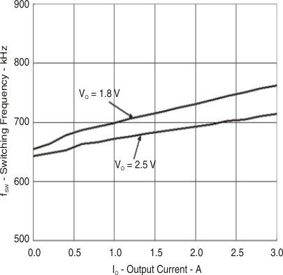
| tON | On time | VIN = 12 V, VO = 1.05 V | 145 | ns | ||
| tOFF(MIN) | Minimum off time | TA = 25°C, VFB = 0.7 V | 260 | ns | ||
| SOFT START | ||||||
| ISSC | SS charge current | VSS = 0 V | 1.4 | 2.0 | 2.6 | μA |
| ISSD | SS discharge current | VSS = 0.5 V | 0.1 | 0.2 | mA | |
| POWER GOOD | ||||||
| VTHPG | PG threshold | VFB rising (good) | 85% | 90% | 95% | |
| VFB falling (fault) | 85% | |||||
| IPG | PG sink current | PG = 0.5 V | 2.5 | 5 | mA | |
| OUTPUT UNDERVOLTAGE AND OVERVOLTAGE PROTECTION | ||||||
| VOVP | Output OVP trip threshold | OVP detect | 115% | 120% | 125% | |
| TOVPDEL | Output OVP prop delay | 5 | μs | |||
| VUVP | Output UVP trip threshold | UVP detect | 65% | 70% | 75% | |
| Hysteresis | 10% | |||||
| TUVPDEL | Output UVP delay | 0.25 | ms | |||
| TUVPEN | Output UVP enable delay | Relative to soft-start time | x 1.7 | |||
| UVLO | ||||||
| VUVLO | UVLO threshold | Wake up VREG5 voltage | 3.45 | 3.70 | 3.95 | V |
| Hysteresis VREG5 voltage | 0.15 | 0.25 | 0.35 | |||
(1) Not production tested.