SLVSC39D November 2013 – January 2017 TPS54361
PRODUCTION DATA.
- 1 Features
- 2 Applications
- 3 Description
- 4 Revision History
- 5 Pin Configuration and Functions
- 6 Specifications
-
7 Detailed Description
- 7.1 Overview
- 7.2 Functional Block Diagram
- 7.3
Feature Description
- 7.3.1 Fixed-Frequency PWM Control
- 7.3.2 Slope Compensation Output Current
- 7.3.3 Pulse-Skip Eco-Mode
- 7.3.4 Low Dropout Operation and Bootstrap Voltage (BOOT)
- 7.3.5 Error Amplifier
- 7.3.6 Adjusting the Output Voltage
- 7.3.7 Enable and Adjust Undervoltage Lockout
- 7.3.8 Soft-Start/Tracking Pin (SS/TR)
- 7.3.9 Sequencing
- 7.3.10 Constant Switching Frequency and Timing Resistor (RT/CLK) Pin)
- 7.3.11 Synchronization to RT/CLK Pin
- 7.3.12 Maximum Switching Frequency
- 7.3.13 Accurate Current Limit Operation
- 7.3.14 Power Good (PWRGD Pin)
- 7.3.15 Overvoltage Protection
- 7.3.16 Thermal Shutdown
- 7.3.17 Small Signal Model for Loop Response
- 7.3.18 Simple Small Signal Model for Peak Current Mode Control
- 7.3.19 Small Signal Model for Frequency Compensation
- 7.4 Device Functional Modes
-
8 Application and Implementation
- 8.1 Application Information
- 8.2
Typical Applications
- 8.2.1
Buck Converter With 7-V to 60-V Input and 5-V at 3.5-A Output
- 8.2.1.1 Design Requirements
- 8.2.1.2
Detailed Design Procedure
- 8.2.1.2.1 Custom Design with WEBENCH® Tools
- 8.2.1.2.2 Selecting the Switching Frequency
- 8.2.1.2.3 Output Inductor Selection (LO)
- 8.2.1.2.4 Output Capacitor
- 8.2.1.2.5 Catch Diode
- 8.2.1.2.6 Input Capacitor
- 8.2.1.2.7 Soft-Start Capacitor
- 8.2.1.2.8 Bootstrap Capacitor Selection
- 8.2.1.2.9 Undervoltage Lockout Set Point
- 8.2.1.2.10 Output Voltage and Feedback Resistors Selection
- 8.2.1.2.11 Compensation
- 8.2.1.2.12 Power Dissipation Estimate
- 8.2.1.2.13 Discontinuous Conduction Mode and Eco-Mode Boundary
- 8.2.1.3 Application Curves
- 8.2.2 Inverting Power Supply
- 8.2.3 Split-Rail Power Supply
- 8.2.1
Buck Converter With 7-V to 60-V Input and 5-V at 3.5-A Output
- 9 Power Supply Recommendations
- 10Layout
- 11Device and Documentation Support
- 12Mechanical, Packaging, and Orderable Information
Package Options
Mechanical Data (Package|Pins)
- DPR|10
Thermal pad, mechanical data (Package|Pins)
- DPR|10
Orderable Information
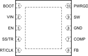
5 Pin Configuration and Functions
DPR Package
10-Pin WSON With Thermal Pad
Top View

Pin Functions
| PIN | I/O | DESCRIPTION | ||
|---|---|---|---|---|
| NAME | NO. | |||
| BOOT | 1 | I | A bootstrap capacitor is required between the BOOT and SW pin. If the voltage on this capacitor is below the minimum required to turn on the high-side MOSFET, the gate drive is switched off until the capacitor is refreshed. | |
| COMP | 7 | I | This pin is the error amplifier output and input to the output switch current (PWM) comparator. Connect frequency compensation components to this pin. | |
| EN | 3 | I | This pin is the enable pin. An internal pullup current source enables the TPS54361 if the EN pin is floating. Pull EN below 1.2 V to disable. Adjust the input undervoltage lockout with two resistors. See Enable and Adjusting Undervoltage Lockout. | |
| FB | 6 | I | This pin is the inverting input of the transconductance (gm) error amplifier. | |
| GND | 8 | – | Ground | |
| PWRGD | 10 | O | The Power Good pin is an open drain output that asserts low if the output voltage is out of regulation because of thermal shutdown, dropout, overvoltage, or EN shutdown. | |
| RT/CLK | 5 | I | This pin is the resistor timing and external clock pin. An internal amplifier holds this pin at a fixed voltage when using an external resistor to ground to set the switching frequency. If the pin is pulled above the PLL upper threshold, a mode change occurs and the pin becomes a synchronization input. The internal amplifier is disabled and the pin is a high-impedance clock input to the internal PLL. If clocking edges stop, the internal amplifier is re-enabled and the operating mode returns to resistor frequency programming. | |
| SS/TR | 4 | I | This pin is the soft start and tracking pin. An external capacitor connected to this pin sets the output rise time. Because the voltage on this pin overrides the internal reference, the SS/TR pin can be used for tracking and sequencing. | |
| SW | 9 | O | The SW pin is the source of the internal high-side power MOSFET and switching node of the converter. | |
| VIN | 2 | I | Connect to this pin the input voltage supply with a 4.5-V to 60-V operating range. | |
| Thermal Pad | – | The GND pin must be electrically connected to the exposed pad on the printed circuit board for proper operation. | ||