SLUSDR5C May 2020 – June 2021 TPS543620
PRODUCTION DATA
- 1 Features
- 2 Applications
- 3 Description
- 4 Revision History
- 5 Pin Configuration and Functions
- 6 Specifications
-
7 Detailed Description
- 7.1 Overview
- 7.2 Functional Block Diagram
- 7.3
Feature Description
- 7.3.1 VIN Pins and VIN UVLO
- 7.3.2 Enable and Adjustable UVLO
- 7.3.3 Adjusting the Output Voltage
- 7.3.4 Switching Frequency Selection
- 7.3.5 Switching Frequency Synchronization to an External Clock
- 7.3.6 Ramp Amplitude Selection
- 7.3.7 Soft Start and Prebiased Output Start-up
- 7.3.8 Mode Pin
- 7.3.9 Power Good (PGOOD)
- 7.3.10 Current Protection
- 7.3.11 Output Overvoltage and Undervoltage Protection
- 7.3.12 Overtemperature Protection
- 7.3.13 Output Voltage Discharge
- 7.3.14 Low-Side MOSFET Resistance Scaling
- 7.4 Device Functional Modes
-
8 Application and Implementation
- 8.1 Application Information
- 8.2
Typical Applications
- 8.2.1
1.0-V Output, 1-MHz Application
- 8.2.1.1 Design Requirements
- 8.2.1.2
Detailed Design Procedure
- 8.2.1.2.1 Switching Frequency
- 8.2.1.2.2 Output Inductor Selection
- 8.2.1.2.3 Output Capacitor
- 8.2.1.2.4 Input Capacitor
- 8.2.1.2.5 Adjustable Undervoltage Lockout
- 8.2.1.2.6 Output Voltage Resistors Selection
- 8.2.1.2.7 Bootstrap Capacitor Selection
- 8.2.1.2.8 BP5 Capacitor Selection
- 8.2.1.2.9 PGOOD Pullup Resistor
- 8.2.1.2.10 Current Limit Selection
- 8.2.1.2.11 Soft-Start Time Selection
- 8.2.1.2.12 Ramp Selection and Control Loop Stability
- 8.2.1.2.13 MODE Pin
- 8.2.1.3 Application Curves
- 8.2.2 1.0-V Output, 1.5-MHz Application
- 8.2.3 3.3-V Output, 1.0-MHz Application
- 8.2.4 1.8-V Output, 1.0-MHz Typical Application
- 8.2.5 5.0-V Output, 1.0-MHz Typical Application
- 8.2.1
1.0-V Output, 1-MHz Application
- 9 Power Supply Recommendations
- 10Layout
- 11Device and Documentation Support
- 12Mechanical, Packaging, and Orderable Information
Package Options
Mechanical Data (Package|Pins)
- RPY|14
Thermal pad, mechanical data (Package|Pins)
Orderable Information
3 Description
The TPS543620 is a high-efficiency 18-V, 6-A synchronous buck converter employing an internally-compensated, fixed-frequency Advanced Current Mode control. It is capable of providing high efficiency while running at a switching frequency up to 2.2 MHz. The device is in a small 2.5-mm x 3-mm HotRod™ VQFN package, which coupled with high efficiency at high frequency, makes it optimal for designs requiring a small solution size. The fixed frequency controller can operate from 500 kHz to 2.2 MHz and can be synchronized to an external clock using the SYNC pin. Additional features include a high accuracy voltage reference, selectable soft start times, montonic start-up into pre-biased outputs, selectable current limits, adjustable UVLO through the EN pin, and a full suite of fault protections.
| PART NUMBER | PACKAGE(1) | BODY SIZE (NOM) |
|---|---|---|
| TPS543620 | VQFN-HR (14) | 2.50 mm x 3.00 mm |
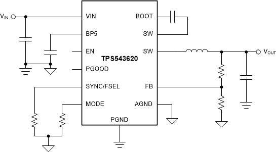
 Simplified Schematic
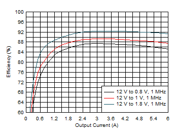
 Efficiency