SLVSB82B May   2012  – April 2021 TPS54525

PRODUCTION DATA  

  1. Features
  2. Applications
  3. Description
  4. Revision History
  5. Pin Configuration and Functions
  6. Specifications
    1. 6.1 Absolute Maximum Ratings
    2. 6.2 ESD Ratings
    3. 6.3 Recommended Operating Conditions
    4. 6.4 Thermal Information
    5. 6.5 Electrical Characteristics
    6. 6.6 Typical Characteristics
  7. Detailed Description
    1. 7.1 Overview
    2. 7.2 Functional Block Diagram
    3. 7.3 Feature Description
      1. 7.3.1  PWM Operation
      2. 7.3.2  PWM Frequency and Adaptive On-Time Control
      3. 7.3.3  Soft Start and Pre-Biased Soft Start
      4. 7.3.4  Power Good
      5. 7.3.5  VREG5
      6. 7.3.6  Output Discharge Control
      7. 7.3.7  Current Protection
      8. 7.3.8  Over/Under Voltage Protection
      9. 7.3.9  UVLO Protection
      10. 7.3.10 Thermal Shutdown
    4. 7.4 Device Functional Modes
      1. 7.4.1 Forced CCM Mode
  8. Application and Implementation
    1. 8.1 Application Information
    2. 8.2 Typical Application
      1. 8.2.1 Design Requirements
      2. 8.2.2 Detailed Design Procedure
        1. 8.2.2.1 Step By Step Design Procedure
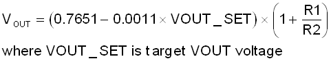
        2. 8.2.2.2 Output Voltage Resistors Selection
        3. 8.2.2.3 Output Filter Selection
        4. 8.2.2.4 Input Capacitor Selection
        5. 8.2.2.5 Bootstrap Capacitor Selection
        6. 8.2.2.6 VREG5 Capacitor Selection
      3. 8.2.3 Application Curves
  9. Power Supply Recommendations
  10. 10Layout
    1. 10.1 Layout Guidelines
    2. 10.2 Layout Guidelines
      1. 10.2.1 Thermal Considerations
  11. 11Device and Documentation Support
    1. 11.1 Device Support
      1. 11.1.1 Third-Party Products Disclaimer
    2. 11.2 Receiving Notification of Documentation Updates
    3. 11.3 Support Resources
    4. 11.4 Trademarks
    5. 11.5 Electrostatic Discharge Caution
    6. 11.6 Glossary

Package Options

Mechanical Data (Package|Pins)
Thermal pad, mechanical data (Package|Pins)
Orderable Information

Output Voltage Resistors Selection

The output voltage is set with a resistor divider from the output node to the VFB pin. It is recommended to use 1% tolerance or better divider resistors. Start by using Equation 2 to calculate VOUT.

To improve efficiency at very light loads consider using larger value resistors, too high of resistance will be more susceptible to noise and voltage errors from the VFB input current will be more noticeable.

Equation 2. GUID-4D0956AD-3D92-4C0B-B996-319CEE7D8F7D-low.gif