SLVS398H June   2001  – October 2015 TPS54610

PRODUCTION DATA.  

  1. Features
  2. Applications
  3. Description
    1.     Device Images
      1.      Simplified Schematic
      2.      Efficiency at 350 kHz
  4. Revision History
  5. Device Comparison Table
  6. Pin Configuration and Functions
    1.     Pin Functions
  7. Specifications
    1. 7.1 Absolute Maximum Ratings
    2. 7.2 ESD Ratings
    3. 7.3 Recommended Operating Conditions
    4. 7.4 Thermal Information
    5. 7.5 Electrical Characteristics
    6. 7.6 Dissipation Ratings
    7. 7.7 Typical Characteristics
  8. Detailed Description
    1. 8.1 Overview
    2. 8.2 Functional Block Diagram
    3. 8.3 Feature Description
      1. 8.3.1  Undervoltage Lockout (UVLO)
      2. 8.3.2  Slow Start/Enable (SS/ENA)
      3. 8.3.3  VBIAS Regulator (VBIAS)
      4. 8.3.4  Voltage Reference
      5. 8.3.5  Oscillator and PWM Ramp
      6. 8.3.6  Error Amplifier
      7. 8.3.7  PWM Control
      8. 8.3.8  Dead-Time Control and MOSFET Drivers
      9. 8.3.9  Overcurrent Protection
      10. 8.3.10 Thermal Shutdown
      11. 8.3.11 Power-Good (PWRGD)
    4. 8.4 Device Functional Modes
      1. 8.4.1 Continuous Conduction Mode
      2. 8.4.2 Switching Frequency Selection/Synchronization
  9. Application and Implementation
    1. 9.1 Application Information
    2. 9.2 Typical Applications
      1. 9.2.1 High Frequency Switching Regulator Using Ceramic Output Capacitors
        1. 9.2.1.1 Design Requirements
        2. 9.2.1.2 Detailed Design Procedure
          1. 9.2.1.2.1 Component Selection
          2. 9.2.1.2.2 Input Filter
          3. 9.2.1.2.3 Feedback Circuit
          4. 9.2.1.2.4 Operating Frequency
          5. 9.2.1.2.5 Output Filter
        3. 9.2.1.3 Application Curves
      2. 9.2.2 High Frequency Application
        1. 9.2.2.1 Design Requirements
        2. 9.2.2.2 Detailed Design Procedure
        3. 9.2.2.3 Application Curve
  10. 10Power Supply Recommendations
  11. 11Layout
    1. 11.1 Layout Guidelines
    2. 11.2 Layout Example
    3. 11.3 Thermal Considerations
  12. 12Device and Documentation Support
    1. 12.1 Device Support
      1. 12.1.1 Related DC/DC Products
    2. 12.2 Receiving Notification of Documentation Updates
    3. 12.3 Community Resources
    4. 12.4 Trademarks
    5. 12.5 Electrostatic Discharge Caution
    6. 12.6 Glossary
  13. 13Mechanical, Packaging, and Orderable Information

Package Options

Mechanical Data (Package|Pins)
Thermal pad, mechanical data (Package|Pins)
Orderable Information

High Frequency Application

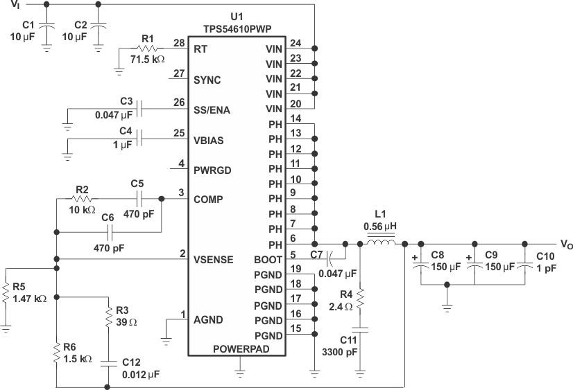
Figure 20 shows the schematic diagram for a reduced size, high frequency application using the TPS54610. The TPS54610 (U1) can provide up to 6 A of output current at a nominal outputvoltage of 1.8 V. A small size 0.56 uH inductor is used and the switching frequency is set to 680 kHz by R1. The compensation network is optimized for fast transient response as shown in Figure 20.
TPS54610 dg_hf_dsg_lvs398.gifFigure 20. Small Size, High Frequency Design