SNVSBV3A July 2021 – July 2021 TPS548B27
PRODUCTION DATA
- 1 Features
- 2 Applications
- 3 Description
- 4 Revision History
- 5 Pin Configuration and Functions
- 6 Specifications
-
7 Detailed Description
- 7.1 Overview
- 7.2 Functional Block Diagram
- 7.3
Feature Description
- 7.3.1 Internal VCC LDO and Using External Bias on VCC Pin
- 7.3.2 Enable
- 7.3.3 Output Voltage Setting
- 7.3.4 Internal Fixed Soft Start and External Adjustable Soft Start
- 7.3.5 External REFIN For Output Voltage Tracking
- 7.3.6 Frequency and Operation Mode Selection
- 7.3.7 D-CAP3 Control
- 7.3.8 Low-Side FET Zero-Crossing
- 7.3.9 Current Sense and Positive Overcurrent Protection
- 7.3.10 Low-Side FET Negative Current Limit
- 7.3.11 Power Good
- 7.3.12 Overvoltage and Undervoltage Protection
- 7.3.13 Out-Of-Bounds (OOB) Operation
- 7.3.14 Output Voltage Discharge
- 7.3.15 UVLO Protection
- 7.3.16 Thermal Shutdown
- 7.4 Device Functional Modes
-
8 Application and Implementation
- 8.1 Application Information
- 8.2
Typical Application
- 8.2.1 Design Requirements
- 8.2.2
Detailed Design Procedure
- 8.2.2.1 Output Voltage Setting Point
- 8.2.2.2 Choose the Switching Frequency and the Operation Mode
- 8.2.2.3 Choose the Inductor
- 8.2.2.4 Set the Current Limit (TRIP)
- 8.2.2.5 Choose the Output Capacitor
- 8.2.2.6 Choose the Input Capacitors (CIN)
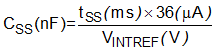
- 8.2.2.7 Soft-Start Capacitor (SS/REFIN Pin)
- 8.2.2.8 EN Pin Resistor Divider
- 8.2.2.9 VCC Bypass Capacitor
- 8.2.2.10 BOOT Capacitor
- 8.2.2.11 PGOOD Pullup Resistor
- 8.2.3 Application Curves
- 9 Power Supply Recommendations
- 10Layout
- 11Device and Documentation Support
- 12Mechanical, Packaging, and Orderable Information
Package Options
Mechanical Data (Package|Pins)
- RYL|19
Thermal pad, mechanical data (Package|Pins)
Orderable Information
7.3.4 Internal Fixed Soft Start and External Adjustable Soft Start
The TPS548B27 implements a circuit to allow both internal fixed soft start and external adjustable soft start. The internal soft-start time is typically 1.5 ms. The soft-start time can be increased by adding a soft-start (SS) capacitor between the SS/REFIN and VSNS– pins. The total SS capacitor value can be determined by Equation 2. The device follows the longer SS ramp among the internal SS time and the SS time determined by the external SS capacitors. The recommended maximum SS capacitor is 1 µF. A minimum 1-nF SS capacitor is required.
The device does not require a capacitor from the SS/REFIN pin to AGND, thus it is not recommended to place a capacitor from the SS/REFIN pin to AGND. If both CSS/REFIN-to-VSNS– and CSS/REFIN-to-AGND capacitors exist, place CSS/REFIN-to-VSNS– more closely with shortest trace back to the VSNS– pin.
The TPS548B27 provides an analog input pin (SS/REFIN) to accept an external reference. When an external voltage signal is applied between the SS/REFIN pin and VSNS– pin, it acts as the reference voltage, thus FB voltage follows this external voltage signal exactly. Applying this external reference to the SS/REFIN pin before the EN high signal is recommended. The external reference must be equal to or higher than the internal reference level to ensure correct power-good thresholds during soft start.
With an external reference applied, the internal fixed soft-start controls the output voltage ramp during start-up. After soft start finishes, the external voltage signal can be in a range of 0.5 V to 1.2 V.
When driving the SS/REFIN pin with an external resistor divider, the resistance should be low enough so that the external voltage source can overdrive the internal current source.