SNVSBC5A December 2020 – December 2022 TPS548B28
PRODUCTION DATA
- 1 Features
- 2 Applications
- 3 Description
- 4 Revision History
- 5 Pin Configuration and Functions
- 6 Specifications
-
7 Detailed Description
- 7.1 Overview
- 7.2 Functional Block Diagram
- 7.3
Feature Description
- 7.3.1 Internal VCC LDO And Using External Bias On VCC Pin
- 7.3.2 Enable
- 7.3.3 Output Voltage Setting
- 7.3.4 Internal Fixed Soft Start and External Adjustable Soft Start
- 7.3.5 External REFIN For Output Voltage Tracking
- 7.3.6 Frequency and Operation Mode Selection
- 7.3.7 D-CAP3™ Control Mode
- 7.3.8 Low-side FET Zero-Crossing
- 7.3.9 Current Sense and Positive Overcurrent Protection
- 7.3.10 Low-side FET Negative Current Limit
- 7.3.11 Power Good
- 7.3.12 Overvoltage and Undervoltage Protection
- 7.3.13 Out-Of-Bounds (OOB) Operation
- 7.3.14 Output Voltage Discharge
- 7.3.15 UVLO Protection
- 7.3.16 Thermal Shutdown
- 7.4 Device Functional Modes
-
8 Application and Implementation
- 8.1 Application Information
- 8.2
Typical Application
- 8.2.1 Design Requirements
- 8.2.2
Detailed Design Procedure
- 8.2.2.1 Output Voltage Setting Point
- 8.2.2.2 Choose the Switching Frequency and the Operation Mode
- 8.2.2.3 Choose the Inductor
- 8.2.2.4 Set the Current Limit (TRIP)
- 8.2.2.5 Choose the Output Capacitor
- 8.2.2.6 Choose the Input Capacitors (CIN)
- 8.2.2.7 Soft Start Capacitor (SS/REFIN Pin)
- 8.2.2.8 EN Pin Resistor Divider
- 8.2.2.9 VCC Bypass Capacitor
- 8.2.2.10 BOOT Capacitor
- 8.2.2.11 PGOOD Pullup Resistor
- 8.2.3 Application Curves
- 8.3 Power Supply Recommendations
- 8.4 Layout
- 9 Device and Documentation Support
- 10Mechanical, Packaging, and Orderable Information
Package Options
Mechanical Data (Package|Pins)
- RWW|21
Thermal pad, mechanical data (Package|Pins)
Orderable Information
7.3.2 Enable
When the EN pin voltage rises above the enable threshold voltage (typically 1.22 V) and VIN rises above the VIN UVLO rising threshold, the device enters its internal power-up sequence. The EN to first switching delay is specified in Start-up section in Section 6.5.
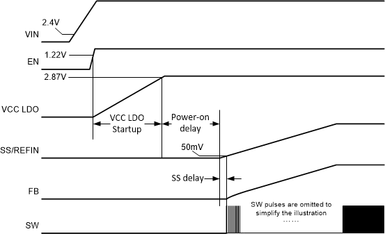
When using the internal VCC LDO, the internal power-up sequence includes three sequential steps. During the first period, the VCC voltage is charged up on a VCC bypass capacitor by an 11-mA current source. The length of this VCC LDO start-up time varies with the capacitance on VCC pin. However, if the VIN voltage ramps up very slowly, the VCC LDO output voltage will be limited by the VIN voltage level, thus the VCC LDO start-up time can be extended longer. Because the VCC LDO start-up time is relatively long, the internal VINTREF build-up happens and finishes during this period. After the VCC voltage crosses above the VCC UVLO rising threshold (typically 2.87 V), the device moves to the second step, power-on delay. The MODE pin setting detection, SS/REFIN pin detection, and control loop initialization are finished within this 285-μs delay. Soft-start ramp starts when the 285-μs power-on delay finishes. During the soft-start ramp power stage, switching does not happen until the SS/REFIN pin voltage reaches 50 mV. This introduces a SS delay that varies with the external capacitance on SS/REFIN pin.
Figure 7-1 shows an example where the VIN UVLO rising threshold is satisfied earlier than the EN rising threshold. In this scenario, the VCC UVLO rising threshold becomes the gating signal to start the internal power-up sequence, and the sequence between VIN and EN does not matter.
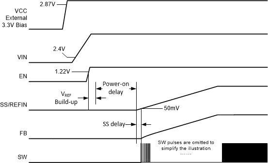
When using an external bias on the VCC pin, the internal power-up sequence still includes three sequential steps. The first period is much shorter because VCC voltage is built up already. A 100-µs period allows the internal references to start up and reach regulation points. This 100-µs period includes not only the 0.6-V VINTREF, but also all of the other reference voltages for various functions. The device then moves to the second step, power-on delay. The MODE pin setting detection, SS/REFIN pin detection, and control loop initialization are finished within this 285-μs delay. Soft-start ramp starts when the 285-μs power-on delay finishes. During the soft-start ramp power stage, switching does not happen until the SS/REFIN pin voltage reaches 50 mV. This introduces a SS delay that varies with the external capacitance on SS/REFIN pin.
Figure 7-2 shows an example where the VIN UVLO rising threshold and EN rising threshold are satisfied later than the VCC UVLO rising threshold. In this scenario, the VIN UVLO rising threshold or EN rising threshold, whoever is satisfied later, becomes the gating signal to start the internal power-up sequence.
 Figure 7-1 Internal Power-up Sequence Using Internal LDO
 Figure 7-2 Internal Power-up Sequence Using External Bias
The EN pin has an internal filter to avoid unexpected ON or OFF due to small glitches. The time constant of this RC filter is 5 µs. For example, when applying 3.3-V voltage source on the EN pin that jumps from 0 V to 3.3 V with an ideal rising edge, the internal EN signal will reach 2.086 V after 5 µs, which is 63.2% of applied 3.3-V voltage level.
A internal pulldown resistor is implemented between the EN pin and AGND pin. To avoid impact to the EN rising/falling threshold, this internal pulldown resistor is set to 6.5 MΩ. With this pulldown resistor, floating the EN pin before start-up keeps the device under disabled state. During nominal operation when the power stage switches, this large internal pulldown resistor can not have enough noise immunity to hold EN pin low.
The recommended operating condition for EN pin is maximum 5.5 V. Do not connect the EN pin to the VIN pin directly.