SLVSH28A december 2022 – april 2023 TPS552892
PRODUCTION DATA
- 1 Features
- 2 Applications
- 3 Description
- 4 Revision History
- 5 Pin Configuration and Functions
- 6 Specifications
-
7 Detailed Description
- 7.1 Overview
- 7.2 Functional Block Diagram
- 7.3
Feature Description
- 7.3.1 VCC Power Supply
- 7.3.2 EXTVCC Power Supply
- 7.3.3 Input Undervoltage Lockout
- 7.3.4 Enable and Programmable UVLO
- 7.3.5 Soft Start
- 7.3.6 Shutdown
- 7.3.7 Switching Frequency
- 7.3.8 Switching Frequency Dithering
- 7.3.9 Inductor Current Limit
- 7.3.10 Internal Charge Path
- 7.3.11 Output Voltage Setting
- 7.3.12 Output Current Monitoring and Cable Voltage Droop Compensation
- 7.3.13 Output Current Limit
- 7.3.14 Overvoltage Protection
- 7.3.15 Output Short Circuit Protection
- 7.3.16 Power Good
- 7.3.17 Constant Current Output Indication
- 7.3.18 Thermal Shutdown
- 7.4 Device Functional Modes
- 8 Application and Implementation
- 9 Device and Documentation Support
- 10Mechanical, Packaging, and Orderable Information
Package Options
Mechanical Data (Package|Pins)
- RYQ|21
Thermal pad, mechanical data (Package|Pins)
- RYQ|21
Orderable Information
7.3.12 Output Current Monitoring and Cable Voltage Droop Compensation
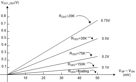
The TPS552892 outputs a voltage at the CDC pin proportional to the sensed voltage across a output current sensing resistor between the ISP pin and the ISN pin. Equation 6 shows the exact voltage at the CDC pin related to the sensed output current.

To compensate the voltage droop across a cable from the output of the USB port to its powered device, the TPS552892 can lift its output voltage in proportion to the load current by placing a resistor between the CDC pin and AGND pin.
The output voltage rises in proportion to the current sourcing from the CDC pin through the resistor at the CDC pin. It is recommended to use 100-kΩ resistance for the up resistor of the feedback resistor divider. Equation 7 shows the output voltage rise related to the sensed output current, the resistance at the CDC pin, and the up resistor of the output voltage feedback resistor divider.

where
- RFB_UP is the up resistor of the resistor divider between the output and the FB pin
- RCDC is the resistor at the CDC pin
When RFB_UP is 100 kΩ, the output voltage rise versus the sensed output current and the resistor at the CDC pin is shown in Figure 7-6.
 Figure 7-6 Output Voltage Rise versus
Output Current