SLVSE22B September   2017  – June 2018 TPS560430

UNLESS OTHERWISE NOTED, this document contains PRODUCTION DATA.  

  1. Features
  2. Applications
  3. Description
    1.     Device Images
      1.      Simplified Schematic
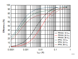
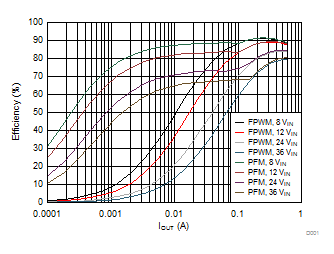
      2.      Efficiency vs Output Current VOUT = 5 V, 1100 kHz, PFM
  4. Revision History
  5. Device Comparison Table
  6. Pin Configuration and Functions
    1.     Pin Functions
  7. Specifications
    1. 7.1 Absolute Maximum Ratings
    2. 7.2 ESD Ratings
    3. 7.3 Recommended Operating Conditions
    4. 7.4 Thermal Information
    5. 7.5 Electrical Characteristics
    6. 7.6 Timing Requirements
    7. 7.7 Switching Characteristics
    8. 7.8 Typical Characteristics
  8. Detailed Description
    1. 8.1 Overview
    2. 8.2 Functional Block Diagram
    3. 8.3 Feature Description
      1. 8.3.1 Fixed Frequency Peak Current Mode Control
      2. 8.3.2 Adjustable Output Voltage
      3. 8.3.3 Enable
      4. 8.3.4 Minimum ON-Time, Minimum OFF-Time and Frequency Foldback
      5. 8.3.5 Bootstrap Voltage
      6. 8.3.6 Over Current and Short Circuit Protection
      7. 8.3.7 Soft Start
      8. 8.3.8 Thermal Shutdown
    4. 8.4 Device Functional Modes
      1. 8.4.1 Shutdown Mode
      2. 8.4.2 Active Mode
      3. 8.4.3 CCM Mode
      4. 8.4.4 Light-Load Operation (PFM Version)
      5. 8.4.5 Light-Load Operation (FPWM Version)
  9. Application and Implementation
    1. 9.1 Application Information
    2. 9.2 Typical Application
      1. 9.2.1 Design Requirements
      2. 9.2.2 Detailed Design Procedure
        1. 9.2.2.1 Custom Design With WEBENCH® Tools
        2. 9.2.2.2 Output Voltage Set-Point
        3. 9.2.2.3 Switching Frequency
        4. 9.2.2.4 Inductor Selection
        5. 9.2.2.5 Output Capacitor Selection
        6. 9.2.2.6 Input Capacitor Selection
        7. 9.2.2.7 Bootstrap Capacitor
        8. 9.2.2.8 Under Voltage Lockout Set-Point
      3. 9.2.3 Application Curves
  10. 10Power Supply Recommendations
  11. 11Layout
    1. 11.1 Layout Guidelines
      1. 11.1.1 Compact Layout for EMI Reduction
      2. 11.1.2 Feedback Resistors
    2. 11.2 Layout Example
  12. 12Device and Documentation Support
    1. 12.1 Device Support
      1. 12.1.1 Development Support
        1. 12.1.1.1 Custom Design With WEBENCH® Tools
    2. 12.2 Documentation Support
      1. 12.2.1 Related Documentation
    3. 12.3 Receiving Notification of Documentation Updates
    4. 12.4 Community Resources
    5. 12.5 Trademarks
    6. 12.6 Electrostatic Discharge Caution
    7. 12.7 Glossary
  13. 13Mechanical, Packaging, and Orderable Information

Package Options

Refer to the PDF data sheet for device specific package drawings

Mechanical Data (Package|Pins)
  • DBV|6
Thermal pad, mechanical data (Package|Pins)
Orderable Information

Typical Characteristics

VIN = 12 V, fSW = 1.1 MHz, TA = 25°C, unless otherwise specified.
TPS560430 D001_updated_SLVSE22.gif
fSW = 1.1 MHz VOUT = 3.3 V
Figure 1. Efficiency vs Load Current
TPS560430 D003_updated_SLVSE22.gif
fSW = 1.1 MHz VOUT = 12 V
Figure 3. Efficiency vs Load Current
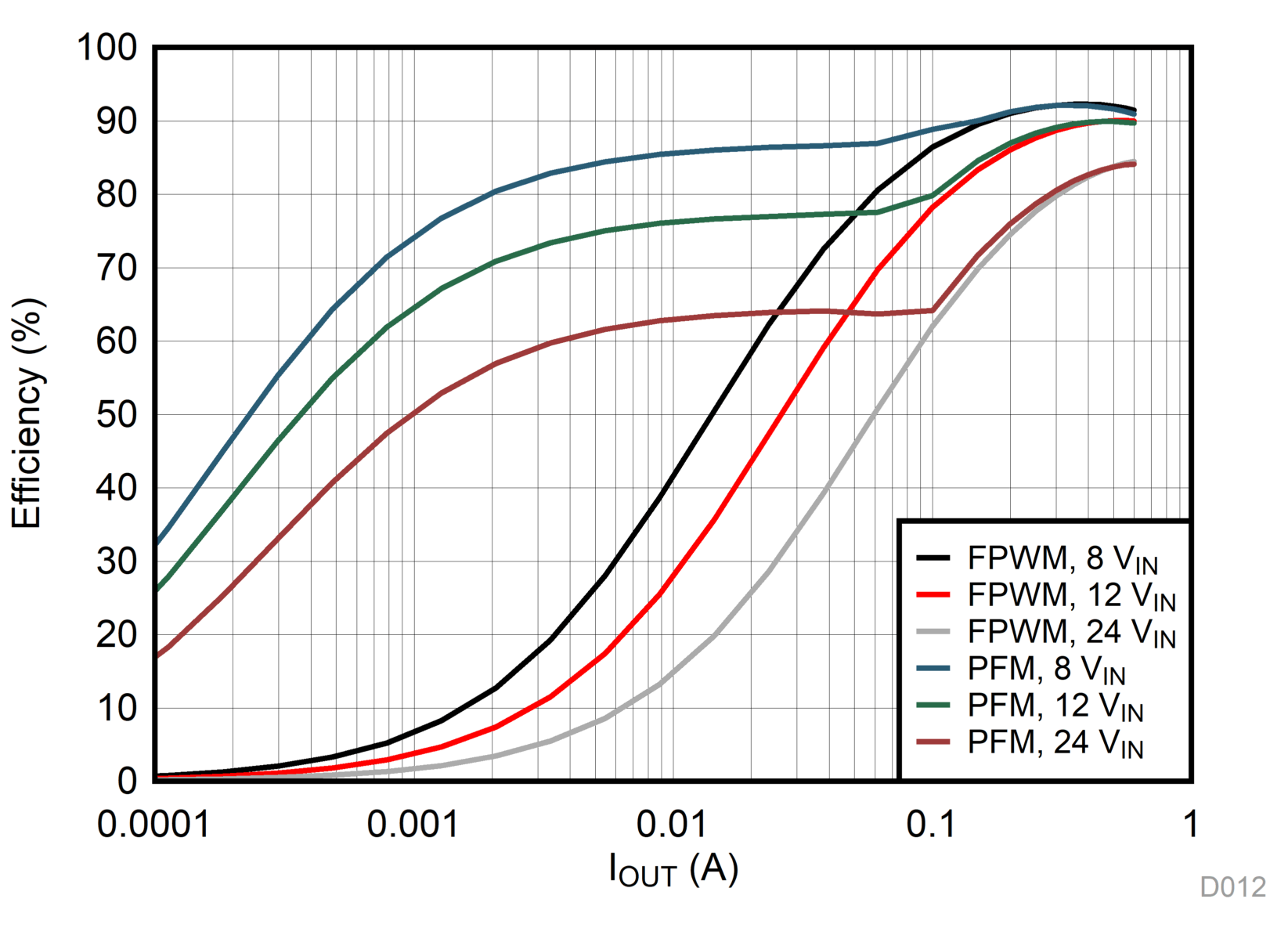
TPS560430 D012_new_SLVSE22.gif
fSW = 2.1 MHz VOUT = 5 V
Figure 5. Efficiency vs Load Current
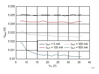
TPS560430 D005_new_SLVSE22.gif
fSW = 1.1 MHz VOUT = 5 V FPWM version
Figure 7. Line Regulation
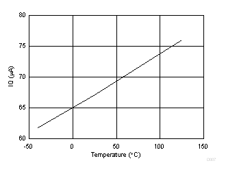
TPS560430 D007_SLVSE22.gif
VFB = 1.1 V PFM verison
Figure 9. IQ vs Temperature
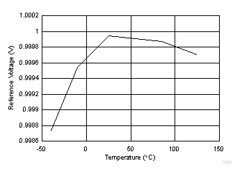
TPS560430 D009_SLVSE22.gif
Figure 11. Reference Voltage vs Temperature
TPS560430 D002_updated_SLVSE22.gif
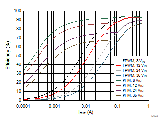
fSW = 1.1 MHz VOUT = 5 V
Figure 2. Efficiency vs Load Current
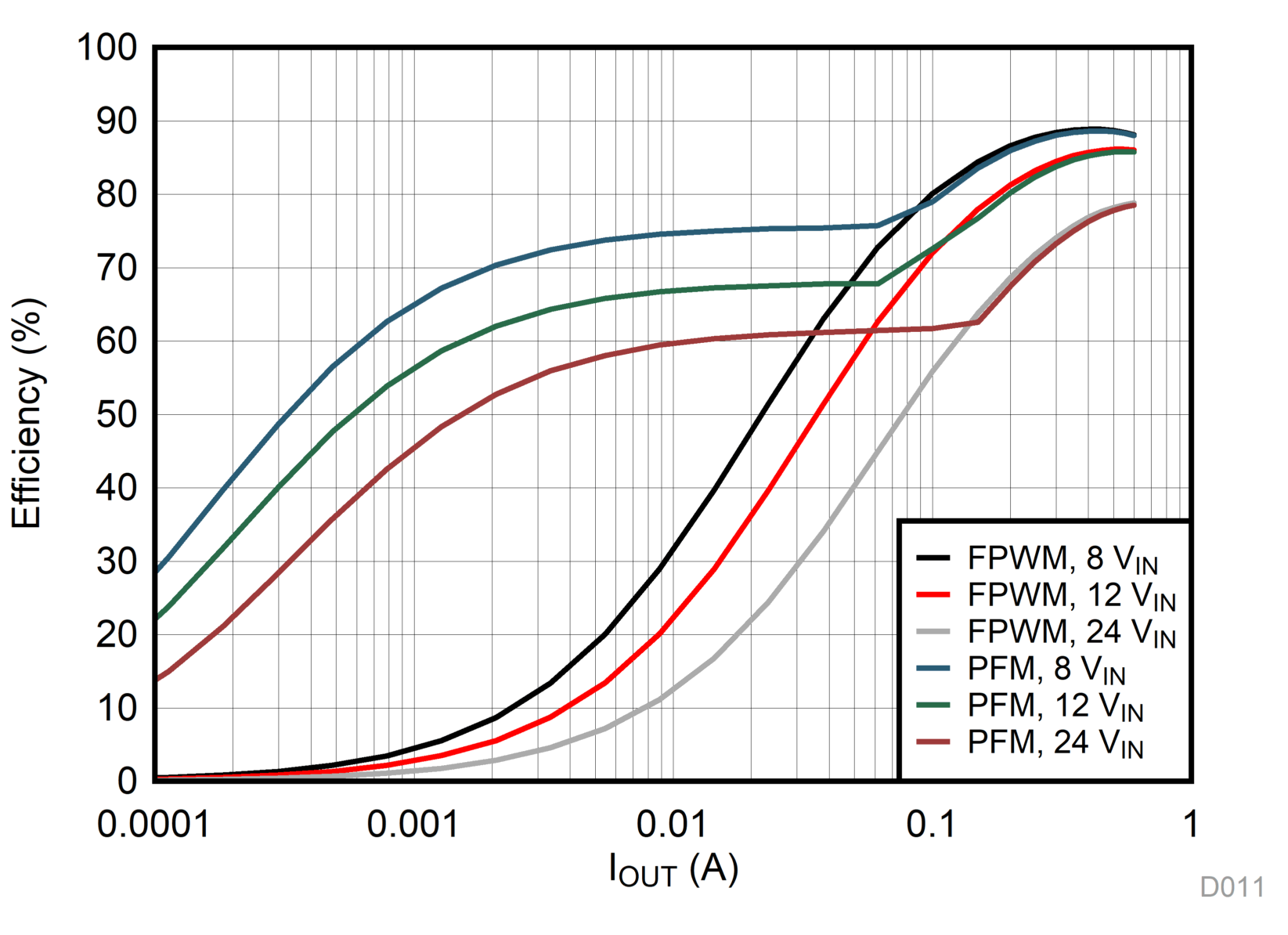
TPS560430 D011_new_SLVSE22.gif
fSW = 2.1 MHz VOUT = 3.3 V
Figure 4. Efficiency vs Load Current
TPS560430 D004_updated_SLVSE22.gif
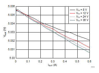
fSW = 1.1 MHz VOUT = 5 V FPWM version
Figure 6. Load Regulation
TPS560430 D006_SLVSE22.gif
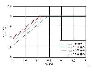
fSW = 1.1 MHz VOUT = 5 V FPWM version
Figure 8. Dropout
TPS560430 D008_SLVSE22.gif
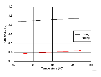
Figure 10. VIN UVLO vs Temperature
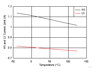
TPS560430 D010_SLVSE22.gif
Figure 12. HS and LS Current Limit vs Temperature