SLVSCM5A September   2014  – November 2016 TPS562209 , TPS563209

PRODUCTION DATA.  

  1. Features
  2. Applications
  3. Description
  4. Revision History
  5. Pin Configuration and Functions
  6. Specifications
    1. 6.1 Absolute Maximum Ratings
    2. 6.2 ESD Ratings
    3. 6.3 Recommended Operating Conditions
    4. 6.4 Thermal Information
    5. 6.5 Electrical Characteristics
    6. 6.6 Typical Characteristics TPS562209
    7. 6.7 Typical Characteristics TPS563209
  7. Detailed Description
    1. 7.1 Overview
    2. 7.2 Functional Block Diagram
    3. 7.3 Feature Description
      1. 7.3.1 The Adaptive On-Time Control and PWM Operation
      2. 7.3.2 Soft Start and Pre-Biased Soft Start
      3. 7.3.3 Current Protection
      4. 7.3.4 Over Voltage Protection
      5. 7.3.5 UVLO Protection
      6. 7.3.6 Thermal Shutdown
    4. 7.4 Device Functional Modes
      1. 7.4.1 Normal Operation
      2. 7.4.2 Forced CCM Operation
      3. 7.4.3 Standby Operation
  8. Application and Implementation
    1. 8.1 Application Information
    2. 8.2 Typical Applications
      1. 8.2.1 TPS562209 4.5-V to 17-V Input, 1.05-V Output Converter
        1. 8.2.1.1 Design Requirements
        2. 8.2.1.2 Detailed Design Procedure
          1. 8.2.1.2.1 Output Voltage Resistors Selection
          2. 8.2.1.2.2 Output Filter Selection
          3. 8.2.1.2.3 Input Capacitor Selection
          4. 8.2.1.2.4 Bootstrap Capacitor Selection
        3. 8.2.1.3 Application Curves
      2. 8.2.2 TPS563209 4.5-V to 17-V Input, 1.05-V Output Converter
        1. 8.2.2.1 Design Requirements
        2. 8.2.2.2 Detailed Design Procedures
          1. 8.2.2.2.1 Output Filter Selection
        3. 8.2.2.3 Application Curves
  9. Power Supply Recommendations
  10. 10Layout
    1. 10.1 Layout Guidelines
    2. 10.2 Layout Example
  11. 11Device and Documentation Support
    1. 11.1 Related Links
    2. 11.2 Receiving Notification of Documentation Updates
    3. 11.3 Community Resources
    4. 11.4 Trademarks
    5. 11.5 Electrostatic Discharge Caution
    6. 11.6 Glossary
  12. 12Mechanical, Packaging, and Orderable Information

Package Options

Mechanical Data (Package|Pins)
Thermal pad, mechanical data (Package|Pins)
Orderable Information

Layout

Layout Guidelines

  1. VIN and GND traces should be as wide as possible to reduce trace impedance. The wide areas are also of advantage from the view point of heat dissipation.
  2. The input capacitor and output capacitor should be placed as close to the device as possible to minimize trace impedance.
  3. Provide sufficient vias for the input capacitor and output capacitor.
  4. Keep the SW trace as physically short and wide as practical to minimize radiated emissions.
  5. Do not allow switching current to flow under the device.
  6. A separate VOUT path should be connected to the upper feedback resistor.
  7. Make a Kelvin connection to the GND pin for the feedback path.
  8. Voltage feedback loop should be placed away from the high-voltage switching trace, and preferably has ground shield.
  9. The trace of the VFB node should be as small as possible to avoid noise coupling.
  10. The GND trace between the output capacitor and the GND pin should be as wide as possible to minimize its trace impedance.

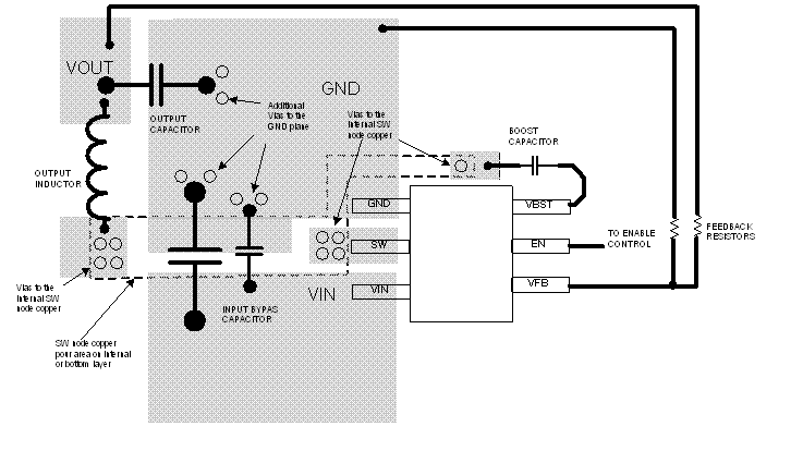
Layout Example

TPS562209 TPS563209 layout_DDC_SLVSCM5.gif Figure 46. TPS562209 and TPS563209 Layout