SLUSDX0A September 2020 – August 2021 TPS562211
PRODUCTION DATA
- 1 Features
- 2 Applications
- 3 Description
- 4 Revision History
- 5 Pin Configuration and Functions
- 6 Specifications
-
7 Detailed Description
- 7.1 Overview
- 7.2 Functional Block Diagram
- 7.3
Feature Description
- 7.3.1 Advanced Emulated Current Mode Control
- 7.3.2 Mode Selection and PG/SS Pin Function Configuration
- 7.3.3 Power Good (PG)
- 7.3.4 Soft Start and Pre-Biased Soft Start
- 7.3.5 Output Discharge through PG/SS Pin
- 7.3.6 Precise Enable and Adjusting Undervoltage Lockout
- 7.3.7 Overcurrent Limit and Undervoltage Protection
- 7.3.8 Overvoltage Protection
- 7.3.9 Thermal Shutdown
- 7.4 Device Functional Modes
- 8 Application and Implementation
- 9 Power Supply Recommendations
- 10Layout
- 11Device and Documentation Support
- 12Mechanical, Packaging, and Orderable Information
Package Options
Mechanical Data (Package|Pins)
- DRL|8
Thermal pad, mechanical data (Package|Pins)
Orderable Information
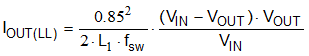
7.4.5 DCM Operation and Eco-Mode Operation
The light load running includes DCM operation and Eco-mode operation.
As the output current decreases from heavy load condition, the inductor current reduces as well and eventually comes to a point that its rippled valley touches zero level, which is the boundary between CCM and DCM. The low-side MOSFET is turned off when the zero inductor current is detected. As the load current further decreases, the converter runs into DCM.
At even lighter current loads, Eco-mode is activated to maintain high efficiency operation. The on time is kept almost the same as it was in CCM so that it takes longer time to discharge the output capacitor with smaller load current to the level of the reference voltage. This makes the switching frequency lower, proportional to the load current, and keeps the light load efficiency high. The transition point to the light load operation, IOUT(LL), current can be calculated in Equation 11.