SLVSCB6E November 2013 – December 2017 TPS56520 , TPS56720 , TPS56920 , TPS56C20
PRODUCTION DATA.
- 1 Features
- 2 Applications
- 3 Description
- 4 Revision History
- 5 Description (Continued)
- 6 Pin Configuration and Functions
- 7 Specifications
- 8 Detailed Description
- 9 Applications and Implementation
- 10Power Supply Recommendations
- 11Layout
- 12Device and Documentation Support
- 13Mechanical, Packaging, and Orderable Information
Package Options
Refer to the PDF data sheet for device specific package drawings
Mechanical Data (Package|Pins)
- PWP|20
Thermal pad, mechanical data (Package|Pins)
- PWP|20
Orderable Information
1 Features
- D-CAP2™ Control
- Input Voltage Range: 4.5V to 17V
- Switching Frequency: 500kHz
- Optimized for a 1.0µH to 2.2µH Inductor
- ±1% Output Voltage Accuracy
- Features via I2C Compatible Interface
- Output Voltage (VID): 0.6V to 1.87V in 10mV
- Auto-Skip Eco-mode™ ON/OFF (Light-load)
- Current Limit Target: 40% to 160%
- Enabling IC, Reading-back Power-good
- Hiccup Mode Protection ON/OFF
- IC Terminal Features
- Start-up by Using External Resistors
Output Voltage with VFB Pin: 0.6V to 1.87V - Adjustable Soft-start,
Monotonic Pre-Biased Start-up - Power-good
- I2C Address Programming (2bits)
- Start-up by Using External Resistors
- Cycle-by-Cycle Overcurrent Limiting Control
- Thermal Shutdown (TSD)
- Undervoltage Lockout (UVLO)
- TSSOP Package (PWP) with PowerPAD™
2 Applications
- Media Processors for Consumer Applications:
Digital TVs, Set Top Boxes (STB, DVD/Blu-ray Player, Cable/Satellite Modem) - SoC Processors
- High Density Power Distribution Systems
3 Description
The TPS56X20 is a synchronous DC-DC converter IC (integrated circuit) with a voltage scaling control to power up micro-processors (MCUs) requiring core voltage (VCORE) tune-ups. After the initial power-up, the output voltage can be programmed/scaled by VID codes sent over an I2C compatible bus.
This step-down (buck) converter employs an adaptive on-time D-CAP2 mode control which provides a very fast transient response with no external components. Unlike traditional voltage-/current-mode controls, the D-CAP2 supports seamless transition between PWM mode for higher load and Eco-mode™ for light load. Eco-mode maintains high efficiency in light-load.
Device Information
| PART NUMBER | PACKAGE | BODY SIZE |
|---|---|---|
| TPS56C20 | HTSSOP (24) | 7.80 mm × 4.40 mm |
| TPS56920 | HTSSOP (20) | 6.50 mm × 4.40 mm |
| TPS56720 | ||
| TPS56520 |
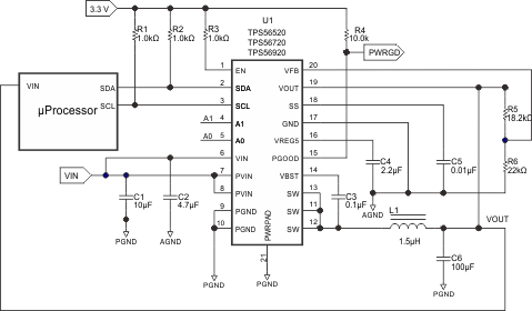
Typical Application Circuit
