SLUSDQ7B May 2020 – December 2023 TPS566231 , TPS566238
PRODUCTION DATA
- 1
- 1 Features
- 2 Applications
- 3 Description
- 4 Pin Configuration and Functions
- 5 Specifications
- 6 Detailed Description
- 7 Application and Implementation
- 8 Device and Documentation Support
- 9 Revision History
- 10Mechanical, Packaging, and Orderable Information
Package Options
Mechanical Data (Package|Pins)
- RQF|9
Thermal pad, mechanical data (Package|Pins)
Orderable Information
3 Description
The TPS56623x are simple, easy-to-use, high-efficiency, 6-A synchronous buck converters in a QFN 9-pin 1.5-mm × 2.0-mm package.
The devices operate with wider supply input voltage ranging from 3 V to 18 V. The D-CAP3 control mode is adopted to provide a fast transient response, good line and load regulation, no requirement for external compensation, and support to low-ESR output capacitors.
The TPS566231 and TPS566231P operate in Eco-mode for high efficiency during light load operation. The devices are designed as the ULQ™ DC/DC converter, achieving 50-μA quiescent current to enable long battery life in low-power applications. The TPS566238 and TPS566238P operate in continuous current mode, which maintains lower output ripple during all load conditions.
The TPS566231 and TPS566238 soft-start time can be adjusted through the SS pin. The TPS566231P and TPS566238P indicate power good through the PG pin.
The TPS56623x can support up to 98% duty cycle operation, and integrate complete protection through OVP, OCP, UVLO, OTP, and UVP with hiccup. The devices are each available in a 9-pin 1.5-mm × 2.0-mm HotRod package. The junction temperature is specified from –40°C to 125°C.
| PART NUMBER |
LIGHT LOAD MODE | PIN-9 DEFINITION |
|---|---|---|
| TPS566231 | Auto-skip mode | Soft-start pin |
| TPS566238 | Continuous current mode | Soft-start pin |
| TPS566231P | Auto-skip mode | Power-good pin |
| TPS566238P | Continuous current mode | Power-good pin |
 Typical Application
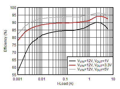
 TPS566231 Efficiency vs Output Current