SLVSCV3B March   2015  – June 2015 TPS566250

PRODUCTION DATA.  

  1. Features
  2. Applications
  3. Description
  4. Simplified Schematic
  5. Revision History
  6. Pin Configuration and Functions
  7. Specifications
    1. 7.1 Absolute Maximum Ratings
    2. 7.2 ESD Ratings
    3. 7.3 Recommended Operating Conditions
    4. 7.4 Thermal Information
    5. 7.5 Electrical Characteristics
    6. 7.6 Timing Requirements
    7. 7.7 Typical Characteristics
  8. Detailed Description
    1. 8.1 Overview
    2. 8.2 Functional Block Diagram
    3. 8.3 Feature Description
      1. 8.3.1 PWM Operation
      2. 8.3.2 PWM Frequency and Adaptive On-Time Control
      3. 8.3.3 Soft Start and Pre-Biased Soft Start
      4. 8.3.4 Overcurrent Protection
      5. 8.3.5 UVLO Protection
      6. 8.3.6 Thermal Shutdown
    4. 8.4 Device Functional Modes
      1. 8.4.1 Auto-Skip Eco-mode™ Control
    5. 8.5 Programming
      1. 8.5.1 I2C Interface
      2. 8.5.2 I2C Protocol
        1. 8.5.2.1 Input Voltage
        2. 8.5.2.2 Output Voltage
        3. 8.5.2.3 Data Format
        4. 8.5.2.4 START and STOP Conditions
      3. 8.5.3 I2C Chip Address Byte
    6. 8.6 Register Maps
      1. 8.6.1 I2C Register Address Byte
        1. 8.6.1.1 Output Voltage Register (offset = 00000000) [reset = 0h]
        2. 8.6.1.2 Power Good State Register (offset = 00011000) [reset = 18h]
      2. 8.6.2 CheckSum Bit
      3. 8.6.3 Output Voltage Registers
      4. 8.6.4 Summary of Default Control Bits
        1. 8.6.4.1 DAC Settle
        2. 8.6.4.2 Operation During VID Transition
  9. Applications and Implementation
    1. 9.1 Application Information
    2. 9.2 Typical Application
      1. 9.2.1 Design Requirements
      2. 9.2.2 Detailed Design Procedure
        1. 9.2.2.1 Output Voltage Resistors Selection
        2. 9.2.2.2 Output Filter Selection
        3. 9.2.2.3 Input Capacitor Selection
        4. 9.2.2.4 Bootstrap Capacitor Selection
      3. 9.2.3 Application Performance Curves
  10. 10Power Supply Recommendations
  11. 11Layout
    1. 11.1 Layout Guidelines
    2. 11.2 Layout Example
  12. 12Device and Documentation Support
    1. 12.1 Documentation Support
    2. 12.2 Third-Party Products Disclaimer
    3. 12.3 Community Resources
    4. 12.4 Trademarks
    5. 12.5 Electrostatic Discharge Caution
    6. 12.6 Glossary
  13. 13Mechanical, Packaging, and Orderable Information
    1. 13.1 Thermal Information

Package Options

Mechanical Data (Package|Pins)
Thermal pad, mechanical data (Package|Pins)
Orderable Information

11 Layout

11.1 Layout Guidelines

  • Keep the input switching current loop as small as possible.
  • Keep the SW node as physically small and short as possible to minimize parasitic capacitance and inductance and to minimize radiated emissions. Kelvin connections should be brought from the output to the feedback terminal of the device.
  • Keep analog and non-switching components away from switching components.
  • Make a single point connection from the signal ground to power ground
  • Keep the pattern lines for VIN and GND broad.
  • Exposed pad of device must be connected to GND with solder.
  • Output capacitor should be connected to a broad pattern of the GND.
  • Voltage feedback loop should be as short as possible, and preferably with ground shield.
  • Kelvin connections should be brought from the output to the feedback terminal of the device.
  • Providing sufficient via is preferable for VIN, SW and GND connection.
  • PCB pattern for VIN, SW, and GND should be as broad as possible.
  • Input capacitors should be placed as near as possible to the device.
  • If possible, it is preferred not to allow switching current to flow under the device

11.2 Layout Example
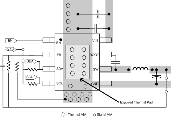
TPS566250 layout_slvscf3.gifFigure 37. Layout