SLVSDI8C october 2016 – august 2023 TPS568215
PRODUCTION DATA
- 1
- 1 Features
- 2 Applications
- 3 Description
- 4 Revision History
- 5 Pin Configuration and Functions
- 6 Specifications
-
7 Detailed Description
- 7.1 Overview
- 7.2 Functional Block Diagram
- 7.3
Feature Description
- 7.3.1 PWM Operation and D-CAP3 Control Mode
- 7.3.2 Eco-mode Control
- 7.3.3 4.7 V LDO and External Bias
- 7.3.4 MODE Selection
- 7.3.5 Soft Start and Pre-biased Soft Start
- 7.3.6 Enable and Adjustable UVLO
- 7.3.7 Power Good
- 7.3.8 Overcurrent Protection and Undervoltage Protection
- 7.3.9 Out-of-Bounds Operation
- 7.3.10 UVLO Protection
- 7.3.11 Thermal Shutdown
- 7.3.12 Output Voltage Discharge
- 7.4 Device Functional Modes
- 8 Application and Implementation
- 9 Device and Documentation Support
- 10Mechanical, Packaging, and Orderable Information
Package Options
Mechanical Data (Package|Pins)
- RNN|18
Thermal pad, mechanical data (Package|Pins)
Orderable Information
7.3.6 Enable and Adjustable UVLO
The EN pin controls the turn-on and turn-off of the device. When EN pin voltage is above the turn-on threshold which is around 1.2 V, the device starts switching and when the EN pin voltage falls below the turn-off threshold which is around 1.1V it stops switching. If the user application requires a different turn-on (VSTART) and turn-off thresholds (VSTOP) respectively, the EN pin can be configured as shown in Figure 7-2 by connecting a resistor divider between VIN and EN. The EN pin has a pull-up current Ip1 that sets the default state of the pin when it is floating. This current increases to Ip2 when the EN pin voltage crosses the turn-on threshold. The UVLO thresholds can be set by using Equation 4 and Equation 5.
 Figure 7-2 Adjustable VIN Under Voltage Lock Out
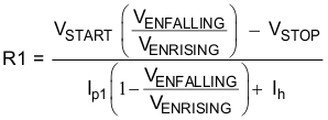
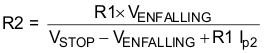
where
- Ip2 = 4.197 μA
- Ip1 = 1.91 μA
- Ih = 2.287 μA
- VENRISING = 1.225 V
- VENFALLING = 1.104 V