SLVSCG0 July 2014 TPS57114-EP
PRODUCTION DATA.
- 1 Features
- 2 Applications
- 3 Description
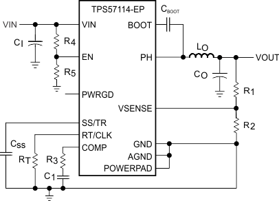
- 4 Simplified Schematic
- 5 Revision History
- 6 Description (continued)
- 7 Pin Configuration and Functions
- 8 Specifications
-
9 Detailed Description
- 9.1 Overview
- 9.2 Functional Block Diagram
- 9.3
Feature Description
- 9.3.1 Fixed-Frequency Pwm Control
- 9.3.2 Slope Compensation and Output Current
- 9.3.3 Bootstrap Voltage (Boot) and Low-Dropout Operation
- 9.3.4 Error Amplifier
- 9.3.5 Voltage Reference
- 9.3.6 Adjusting the Output Voltage
- 9.3.7 Enable Functionality and Adjusting UVLO
- 9.3.8 Slow-Start or Tracking Pin
- 9.3.9 Constant Switching Frequency and Timing Resistor (RT/CLK Pin)
- 9.3.10 Overcurrent Protection
- 9.3.11 Frequency Shift
- 9.3.12 Reverse Overcurrent Protection
- 9.3.13 Synchronize Using the RT/CLK Pin
- 9.3.14 Power Good (PWRGD Pin)
- 9.3.15 Overvoltage Transient Protection (OVTP)
- 9.3.16 Thermal Shutdown
- 9.3.17 Small-Signal Model for Loop Response
- 9.3.18 Simple Small-Signal Model for Peak-Current Mode Control
- 9.3.19 Small-Signal Model for Frequency Compensation
- 9.4 Device Functional Modes
-
10Application and Implementation
- 10.1 Application Information
- 10.2
Typical Application
- 10.2.1 Design Requirements
- 10.2.2
Detailed Design Procedure
- 10.2.2.1 Selecting the Switching Frequency
- 10.2.2.2 Output Inductor Selection
- 10.2.2.3 Output Capacitor
- 10.2.2.4 Input Capacitor
- 10.2.2.5 Slow-Start Capacitor
- 10.2.2.6 Bootstrap Capacitor Selection
- 10.2.2.7 Output-Voltage and Feedback-Resistor Selection
- 10.2.2.8 Compensation
- 10.2.2.9 Power-Dissipation Estimate
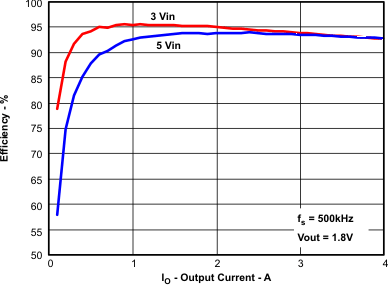
- 10.2.3 Application Curves
- 11Power Supply Recommendations
- 12Layout
- 13Device and Documentation Support
- 14Mechanical, Packaging, and Orderable Information
Package Options
Mechanical Data (Package|Pins)
- RTE|16
Thermal pad, mechanical data (Package|Pins)
- RTE|16
Orderable Information
1 Features
- Two 12-mΩ (Typical) MOSFETs for High Efficiency at 3.5-A Loads
- 200-kHz to 2-MHz Switching Frequency
- 0.8-V ±1% Voltage Reference Over Temperature (–55°C to 125°C)
- Synchronizes to External Clock
- Adjustable Slow Start and Sequencing
- UV and OV Power-Good Output
- Thermally Enhanced 3-mm × 3-mm 16-Pin WQFN
- Supports Defense, Aerospace, and Medical Applications
- Controlled Baseline
- One Assembly and Test Site
- One Fabrication Site
- Available in Military (–55°C to 125°C) Temperature Range
- Extended Product Life Cycle
- Extended Product-Change Notification
- Product Traceability
2 Applications
- Low-Voltage, High-Density Power Systems
- Point-of-Load Regulation for High-Performance DSPs, FPGAs, ASICs, and Microprocessors
- Broadband, Networking, and Optical Communications Infrastructure
3 Description
The TPS57114-EP device is a full-featured 6-V,
3.5-A, synchronous step-down current-mode converter with two integrated MOSFETs.
The TPS57114-EP enables small designs by integrating the MOSFETs, implementing current-mode control to reduce external component count, reducing inductor size by enabling up to 2-MHz switching frequency, and minimizing the IC footprint with a small 3-mm × 3-mm thermally-enhanced WQFN package.
The TPS57114-EP provides accurate regulation for a variety of loads with an accurate ±1% voltage reference (VREF) over temperature.
The integrated 12-mΩ MOSFETs and 515-µA typical supply current maximize efficiency. Entering shutdown mode by using the enable pin reduces the shutdown supply current to 5.5 µA.
The internal undervoltage lockout (UVLO) setting is 2.45 V, but programming the threshold with a resistor network on the enable pin can increase it. The slow-start pin controls the output-voltage start-up ramp. An open-drain power-good signal indicates the output is within 93% to 107% of its nominal voltage.
Device Information(1)
| ORDER NUMBER | PACKAGE | BODY SIZE (NOM) |
|---|---|---|
| TPS57114MRTETEP | WQFN (16) | 3.00 mm × 3.00 mm |
- For all available packages, see the orderable addendum at the end of the data sheet.
4 Simplified Schematic
Efficiency vs Output Current