SLVSD01B September 2015 – May 2019 TPS57140-EP
PRODUCTION DATA.
- 1 Features
- 2 Applications
- 3 Description
- 4 Revision History
- 5 Pin Configuration and Functions
- 6 Specifications
-
7 Detailed Description
- 7.1 Overview
- 7.2 Functional Block Diagram
- 7.3
Feature Description
- 7.3.1 Fixed Frequency PWM Control
- 7.3.2 Slope-Compensation Output Current
- 7.3.3 Bootstrap Voltage (Boot)
- 7.3.4 Low-Dropout Operation
- 7.3.5 Error Amplifier
- 7.3.6 Voltage Reference
- 7.3.7 Adjusting the Output Voltage
- 7.3.8 Enable and Adjusting UVLO
- 7.3.9 Slow-Start or Tracking Pin (SS/TR)
- 7.3.10 Overload Recovery Circuit
- 7.3.11 Constant Switching Frequency and Timing Resistor (RT/CLK Pin)
- 7.3.12 Overcurrent Protection and Frequency Shift
- 7.3.13 Selecting the Switching Frequency
- 7.3.14 How to Interface to RT/CLK Pin
- 7.3.15 Power Good (PWRGD Pin)
- 7.3.16 Overvoltage Transient Protection (OVTP)
- 7.3.17 Thermal Shutdown
- 7.3.18 Small-Signal Model for Loop Response
- 7.3.19 Simple Small-Signal Model for Peak-Current-Mode Control
- 7.3.20 Small-Signal Model for Frequency Compensation
- 7.4 Device Functional Modes
-
8 Application and Implementation
- 8.1 Application Information
- 8.2
Typical Application
- 8.2.1 Design Requirements
- 8.2.2
Detailed Design Procedure
- 8.2.2.1 Selecting the Switching Frequency
- 8.2.2.2 Output Inductor Selection (LO)
- 8.2.2.3 Output Capacitor
- 8.2.2.4 Catch Diode
- 8.2.2.5 Input Capacitor
- 8.2.2.6 Slow-Start Capacitor
- 8.2.2.7 Bootstrap Capacitor Selection
- 8.2.2.8 UVLO Set Point
- 8.2.2.9 Output Voltage and Feedback Resistors Selection
- 8.2.2.10 Compensation
- 8.2.3 Application Curves
- 9 Power Supply Recommendations
- 10Layout
- 11Device and Documentation Support
- 12Mechanical, Packaging, and Orderable Information
Package Options
Mechanical Data (Package|Pins)
- DRC|10
Thermal pad, mechanical data (Package|Pins)
- DRC|10
Orderable Information
7.3.14 How to Interface to RT/CLK Pin
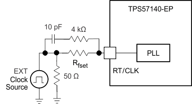
The designer can use the RT/CLK pin to synchronize the regulator to an external system clock. To implement the synchronization feature, connect a square wave to the RT/CLK pin through the circuit network shown in Figure 35. The square wave amplitude must transition lower than 0.5 V and higher than 2.2 V on the RT/CLK pin and have an on-time greater than 40 ns and an off-time greater than 40 ns. The synchronization frequency range is 300 to 2200 kHz. The rising edge of PH synchronizes to the falling edge of the signal on the RT/CLK pin. Design the external synchronization circuit in such a way that the device has the default frequency-set resistor connected from the RT/CLK pin to ground should the synchronization signal turn off. TI recommends using a frequency-set resistor connected as shown in Figure 35 through a 50-Ω resistor to ground. The resistor should set the switching frequency close to the external CLK frequency. TI recommends ac-coupling the synchronization signal through a 10-pF ceramic capacitor and a 4-kΩ series resistor to the RT/CLK pin. The series resistor reduces PH jitter in heavy-load applications when synchronizing to an external clock, and in applications which transition from synchronizing to RT mode. The first time CLK rises above the CLK threshold, the device switches from the RT resistor frequency to PLL mode. The internal 0.5-V voltage source opens and the CLK pin becomes high-impedance as the PLL starts to lock onto the external signal. Because there is a PLL on the regulator, the switching frequency can be higher or lower than the frequency set with the external resistor. The device transitions from the resistor mode to the PLL mode and then increases or decreases the switching frequency until the PLL locks onto the CLK frequency within 100 µs.
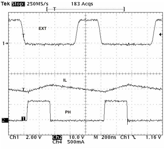
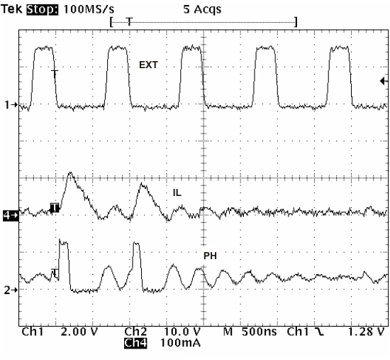
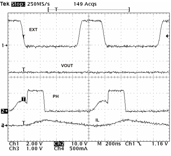
When the device transitions from the PLL to resistor mode, the switching frequency slows down from the CLK frequency to 150 kHz; then reapply the 0.5-V voltage, and the resistor then sets the switching frequency. The divisor of the switching frequency goes to 8, 4, 2, and 1 as the voltage ramps from 0 to 0.8 V on the VSENSE pin. The device implements a digital frequency shift to enable synchronizing to an external clock during normal start-up and fault conditions. Figure 36, Figure 37, and Figure 38 show the device synchronized to an external system clock in continuous-conduction mode (CCM), discontinuous-conduction mode (DCM), and pulse-skip mode (PSM).
 Figure 35. Synchronizing to a System Clock

