SLVS391C October 2001 – September 2015 TPS60500 , TPS60501 , TPS60502 , TPS60503
PRODUCTION DATA.
- 1 Features
- 2 Applications
- 3 Description
- 4 Revision History
- 5 Device Comparison Table
- 6 Pin Configuration and Functions
- 7 Specifications
- 8 Detailed Description
- 9 Application and Implementation
- 10Power Supply Recommendations
- 11Layout
- 12Device and Documentation Support
- 13Mechanical, Packaging, and Orderable Information
Package Options
Mechanical Data (Package|Pins)
- DGS|10
Thermal pad, mechanical data (Package|Pins)
Orderable Information
1 Features
- Wide Input Voltage Range From 1.8 V to 6.5 V
- Regulated 3.3-V, 1.8-V, 1.5-V, or Adjustable Output Voltage
- Up to 250-mA Output Current
- Up to 90% Efficiency
- Output Voltage Tolerance 3% Over Line, Load, and Temperature Variation
- Device Quiescent Current Less Than 40 µA
- Output Voltage Supervisor Included (Power Good)
- Internal Soft Start
- Load Isolated From Battery During Shutdown
- Overtemperature and Overcurrent Protected
- Micro-Small 10-Pin VSSOP Package
- EVM Available, TPS60500EVM-193
2 Applications
- Mobile Phones
- Portable Instruments
- Internet Audio Player
- PC Peripherals
- USB Powered Applications
3 Description
The TPS6050x devices are a family of switched capacitor voltage converters, designed specifically for space-critical battery-powered applications.
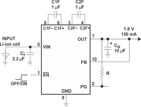
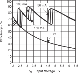
The TPS6050x step-down charge pumps generate a regulated, fixed 3.3-V, 1.8-V, 1.5-V, or adjustable output voltage. Only four small ceramic capacitors are required to build a complete high-efficiency DC–DC charge pump converter. To achieve the high efficiency over a wide input voltage range, the charge pump automatically selects between three different conversion modes. The output can deliver a maximum of 250-mA output current. The power good function supervises the output voltage and goes high when the output voltage rises to 97% of the nominal value.
The TPS6050x devices come in a micro-small 10-pin VSSOP package.
Device Information(1)
| PART NUMBER | PACKAGE | BODY SIZE (NOM) |
|---|---|---|
| TPS60500 TPS60501 TPS60502 TPS60503 |
VSSOP (10) | 3.05 mm × 4.98 mm |
- For all available packages, see the orderable addendum at the end of the data sheet.
Typical Application Schematic

Efficiency vs Input Voltage
