SLVS859B June 2008 – December 2014 TPS61085
PRODUCTION DATA.
- 1 Features
- 2 Applications
- 3 Description
- 4 Simplified Schematic
- 5 Revision History
- 6 Pin Configuration and Functions
- 7 Specifications
- 8 Detailed Description
- 9 Application and Implementation
- 10Power Supply Recommendations
- 11Layout
- 12Device and Documentation Support
- 13Mechanical, Packaging, and Orderable Information
Package Options
Mechanical Data (Package|Pins)
Thermal pad, mechanical data (Package|Pins)
Orderable Information
9 Application and Implementation
NOTE
Information in the following applications sections is not part of the TI component specification, and TI does not warrant its accuracy or completeness. TI’s customers are responsible for determining suitability of components for their purposes. Customers should validate and test their design implementation to confirm system functionality.
9.1 Application Information
The TPS61085 is designed for output voltages up to 18.5 V with a switch peak current limit of 2.0 A minimum. The device, which operates in a current mode scheme with quasi-constant frequency, is externally compensated for maximum flexibility and stability. The switching frequency is selectable between 650 kHz and 1.2 MHz, and the input voltage range is 2.3 V to 6.0V. To control the inrush current at start-up a soft-start pin is available. The following section provides a step-by-step design approach for configuring the TPS61085 as a voltage regulating boost converter.
9.2 Typical Application
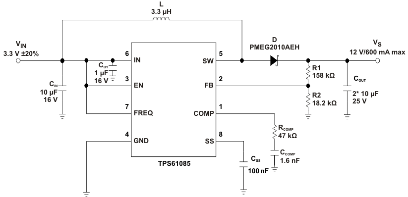
9.2.1 Design Requirements
Table 2. TPS61085 12V Output Design Requirements
| PARAMETERS | VALUES |
|---|---|
| Input Voltage | 3.3V ± 20% |
| Output Voltage | 12V |
| Output Current | 600mA |
| Switching Frequency | 1.2MHz |
9.2.2 Detailed Design Procedure
9.2.2.1 Design Procedure
The first step in the design procedure is to verify that the maximum possible output current of the boost converter supports the specific application requirements. A simple approach is to estimate the converter efficiency, by taking the efficiency numbers from the provided efficiency curves or to use a worst case assumption for the expected efficiency, e.g. 90%.
1. Duty cycle, D:
2. Maximum output current, IOUT(max):
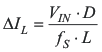
3. Peak switch current in application, ISW(peak):
with the inductor peak-to-peak ripple current, ΔIL
and
| VIN | Minimum input voltage |
| VS | Output voltage |
| ILIM(min) | Converter switch current limit (minimum switch current limit = 3.2 A) |
| fS | Converter switching frequency (typically 1.2 MHz or 650 kHz) |
| L | Selected inductor value |
| η | Estimated converter efficiency (please use the number from the efficiency plots or 90% as an estimation) |
The peak switch current is the steady state peak switch current that the integrated switch, inductor and external Schottky diode has to be able to handle. The calculation must be done for the minimum input voltage where the peak switch current is the highest.
9.2.2.2 Inductor Selection
The TPS61085 is designed to work with a wide range of inductors. The main parameter for the inductor selection is the saturation current of the inductor which should be higher than the peak switch current as calculated in the Design Procedure section with additional margin to cover for heavy load transients. An alternative, more conservative, is to choose an inductor with a saturation current at least as high as the maximum switch current limit of 3.2 A. The other important parameter is the inductor DC resistance. Usually, the lower the DC resistance the higher the efficiency. It is important to note that the inductor DC resistance is not the only parameter determining the efficiency. Especially for a boost converter where the inductor is the energy storage element, the type and core material of the inductor influences the efficiency as well. At high switching frequencies of 1.2 MHz inductor core losses, proximity effects and skin effects become more important. Usually, an inductor with a larger form factor gives higher efficiency. The efficiency difference between different inductors can vary between 2% to 10%. For the TPS61085, inductor values between 3 μH and 6 μH are a good choice with a switching frequency of 1.2 MHz, typically 3.3 μH. At 650 kHz inductors between 6 μH and 13 μH, typically 6.8 μH are recommended. Possible inductors are shown in Table 3.
Typically, it is recommended that the inductor current ripple is below 35% of the average inductor current. Therefore, the following equation can be used to calculate the inductor value, L:
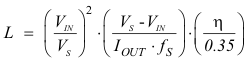
with
| VIN | Minimum input voltage |
| VS | Output voltage |
| Iout | Maximum output current in the application |
| fS | Converter switching frequency (typically 1.2 MHz or 650 kHz) |
| η | Estimated converter efficiency (please use the number from the efficiency plots or 90% as an estimation) |
Table 3. Inductor Selection
| L (μH) |
SUPPLIER | COMPONENT CODE | SIZE (L×W×H mm) |
DCR TYP (mΩ) |
Isat (A) |
|---|---|---|---|---|---|
| 1.2 MHz | |||||
| 3.3 | Sumida | CDH38D09 | 4 x 4 x 1 | 240 | 1.25 |
| 4.7 | Sumida | CDPH36D13 | 5 × 5 × 1.5 | 155 | 1.36 |
| 3.3 | Sumida | CDPH4D19F | 5.2 x 5.2 x 2 | 33 | 1.5 |
| 3.3 | Sumida | CDRH6D12 | 6.7 x 6.7 x 1.5 | 62 | 2.2 |
| 4.7 | Würth Elektronik | 7447785004 | 5.9 × 6.2 × 3.3 | 60 | 2.5 |
| 5 | Coilcraft | MSS7341 | 7.3 × 7.3 × 4.1 | 24 | 2.9 |
| 650 kHz | |||||
| 6.8 | Sumida | CDP14D19 | 5.2 x 5.2 x 2 | 50 | 1 |
| 10 | Coilcraft | LPS4414 | 4.3 × 4.3 × 1.4 | 380 | 1.2 |
| 6.8 | Sumida | CDRH6D12/LD | 6.7 x 6.7 x 1.5 | 95 | 1.25 |
| 10 | Sumida | CDR6D23 | 5 × 5 × 2.4 | 133 | 1.75 |
| 10 | Würth Elektronik | 744778910 | 7.3 × 7.3 × 3.2 | 51 | 2.2 |
| 6.8 | Sumida | CDRH6D26HP | 7 x 7 x 2.8 | 52 | 2.9 |
9.2.2.3 Rectifier Diode Selection
To achieve high efficiency, a Schottky type should be used for the rectifier diode. The reverse voltage rating should be higher than the maximum output voltage of the converter. The averaged rectified forward current Iavg, the Schottky diode needs to be rated for, is equal to the output current IOUT:

Usually a Schottky diode with 2 A maximum average rectified forward current rating is sufficient for most applications. The Schottky rectifier can be selected with lower forward current capability depending on the output current Iout but has to be able to dissipate the power. The dissipated power, PD, is the average rectified forward current times the diode forward voltage, Vforward.
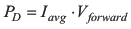
Typically the diode should be able to dissipate around 500mW depending on the load current and forward voltage.
Table 4. Rectifier Diode Selection
| CURRENT RATING Iavg | Vr | Vforward / Iavg | SUPPLIER | COMPONENT CODE | PACKAGE TYPE |
|---|---|---|---|---|---|
| 750 mA | 20 V | 0.425 V / 750 mA | Fairchild Semiconductor | FYV0704S | SOT 23 |
| 1 A | 20 V | 0.39 V / 1 A | NXP | PMEG2010AEH | SOD 123 |
| 1 A | 20 V | 0.52 V / 1 A | Vishay Semiconductor | B120 | SMA |
| 1 A | 20 V | 0.5 V / 1 A | Vishay Semiconductor | SS12 | SMA |
| 1 A | 20 V | 0.44 V / 1 A | Vishay Semiconductor | MSS1P2L | μ-SMP (Low Profile) |
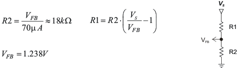
9.2.2.4 Setting the Output Voltage
The output voltage is set by an external resistor divider. Typically, a minimum current of 50 μA flowing through the feedback divider gives good accuracy and noise covering. A standard low side resistor of 18 kΩ is typically selected. The resistors are then calculated as:
9.2.2.5 Compensation (COMP)
The regulator loop can be compensated by adjusting the external components connected to the COMP pin. The COMP pin is the output of the internal transconductance error amplifier.
Standard values of RCOMP = 13 kΩ and CCOMP = 3.3 nF will work for the majority of the applications.
See Table 5 for dedicated compensation networks giving an improved load transient response. The following equations can be used to calculate RCOMP and CCOMP:
with
| VIN | Minimum input voltage |
| VS | Output voltage |
| Cout | Output capacitance |
| L | Inductor value, e.g. 3.3 μH or 6.8 μH |
| IOUT | Maximum output current in the application |
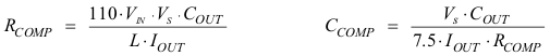
Make sure that RCOMP < 120 kΩ and CCOMP> 820 pF, independent of the results of the above formulas.
Table 5. Recommended Compensation Network Values at High/Low Frequency
| FREQUENCY | L | VS | VIN ± 20% | RCOMP | CCOMP | Used IOUT |
|---|---|---|---|---|---|---|
| High (1.2 MHz) | 3.3 µH | 15 V | 5 V | 82 kΩ | 1.1 nF | 0.7A |
| 3.3 V | 75 kΩ | 1.6 nF | 0.5A | |||
| 12 V | 5 V | 51 kΩ | 1.1 nF | 0.9A | ||
| 3.3 V | 47 kΩ | 1.6 nF | 0.6A | |||
| 9 V | 5 V | 30 kΩ | 1.1 nF | 1.2A | ||
| 3.3 V | 27 kΩ | 1.6 nF | 0.8A | |||
| Low (650 kHz) | 6.8 µH | 15 V | 5 V | 43 kΩ | 2.2 nF | 0.7A |
| 3.3 V | 39 kΩ | 3.3 nF | 0.5A | |||
| 12 V | 5 V | 27 kΩ | 2.2 nF | 0.9A | ||
| 3.3 V | 24 kΩ | 3.3 nF | 0.6A | |||
| 9 V | 5 V | 15 kΩ | 2.2 nF | 1.2A | ||
| 3.3 V | 13 kΩ | 3.3 nF | 0.8A |
Table 5 gives conservative RCOMP and CCOMP values for certain inductors, input and output voltages providing a very stable system. For a faster response time, a higher RCOMP value can be used to enlarge the bandwidth, as well as a slightly lower value of CCOMP to keep enough phase margin. These adjustments should be performed in parallel with the load transient response monitoring of TPS61087.
9.2.2.6 Input Capacitor Selection
For good input voltage filtering low ESR ceramic capacitors are recommended. TPS61085 has an analog input IN. Therefore, a 1 μF bypass is highly recommended as close as possible to the IC from IN to GND.
One 10 μF ceramic input capacitors are sufficient for most of the applications. For better input voltage filtering this value can be increased. Refer to Table 6 and typical applications for input capacitor recommendations.
9.2.2.7 Output Capacitor Selection
For best output voltage filtering a low ESR output capacitor like ceramic capcaitor is recommended. Two 10 μF ceramic output capacitors (or one 22 μF) work for most of the applications. Higher capacitor values can be used to improve the load transient response. Refer to Table 6 for the selection of the output capacitor.
Table 6. Rectifier Input and Output Capacitor Selection
| CAPACITOR | VOLTAGE RATING | SUPPLIER | COMPONENT CODE | |
|---|---|---|---|---|
| CIN | 10 μF/1206 | 16 V | Taiyo Yuden | EMK212 BJ 106KG |
| IN bypass | 1 μF/0603 | 16 V | Taiyo Yuden | EMK107 BJ 105KA |
| COUT | 10 μF/1206 | 25 V | Taiyo Yuden | TMK316 BJ 106KL |
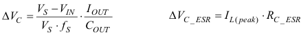
To calculate the output voltage ripple, Equation 10 can be used:
with
| ΔVC | Output voltage ripple dependent on output capacitance,output current and switching frequency |
| VS | Output voltage |
| VIN | Minimum input voltage of boost converter |
| fS | Converter switching frequency (typically 1.2 MHz or 650 kHz) |
| Iout | Output capacitance |
| ΔVC_ESR | Output voltage ripple due to output capacitors ESR (equivalent series resistance) |
| ISWPEAK | Inductor peak switch current in the application |
| RC_ESR | Output capacitors equivalent series resistance (ESR) |
ΔVC_ESR can be neglected in many cases since ceramic capacitors provide low ESR.
9.2.3 Application Curves
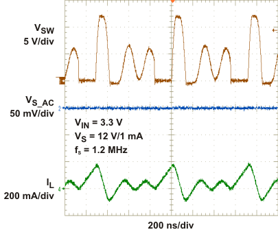 Figure 9. PWM Switching Discontinuous Conduction Mode
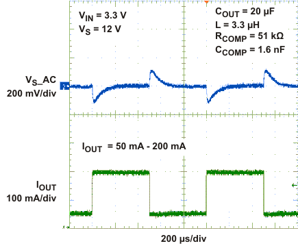 Figure 11. Load Transient Response High Frequency (1.2 MHz)
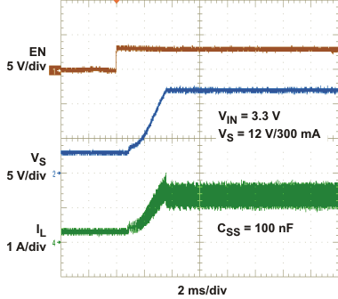 Figure 13. Soft-Start
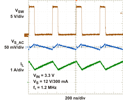 Figure 10. PWM Switching Continuous Conduction Mode
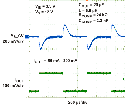 Figure 12. Load Transient Response Low Frequency (650 kHz)
9.3 System Examples
9.3.1 General Boost Application Circuits
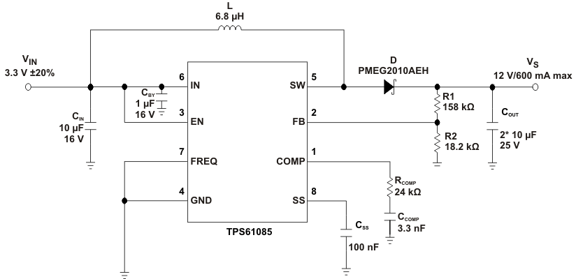 Figure 14. Typical Application, 3.3 V to 12 V (fS = 650 kHz)
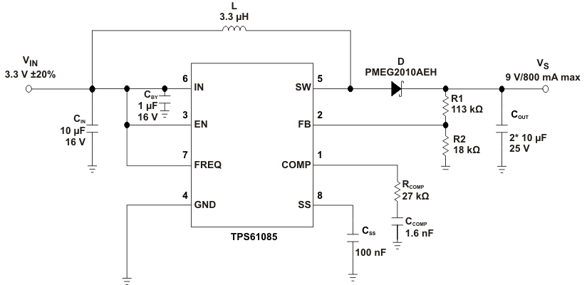 Figure 15. Typical Application, 3.3 V to 9 V (fS = 1.2 MHz)
 Figure 16. Typical Application, 3.3 V to 9 V (fS = 650 kHz)
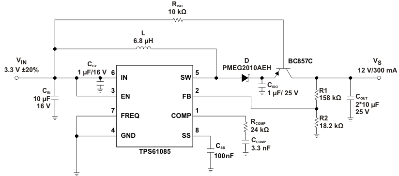 Figure 17. Typical Application With External Load Disconnect Switch
9.3.2 TFT LCD Application Circuit
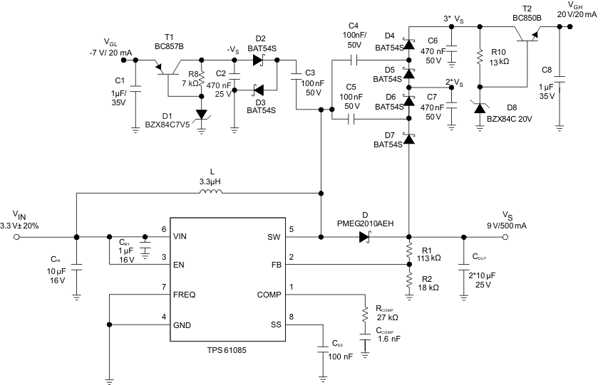 Figure 18. Typical Application 3.3 V to 9 V (fS = 1.2 MHz) for TFT LCD With External Charge Pumps
(VGH, VGL)
9.3.3 WHITE LED Application Circuits
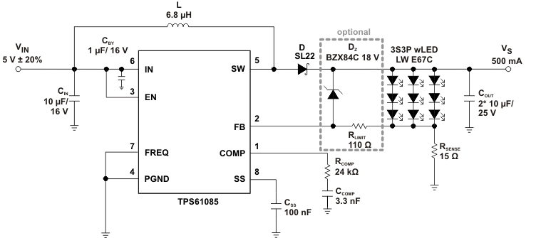 Figure 19. Simple Application (3.3 V Input - fsw = 650 kHz) for wLED Supply (3S3P)
(With Optional Clamping Zener Diode)
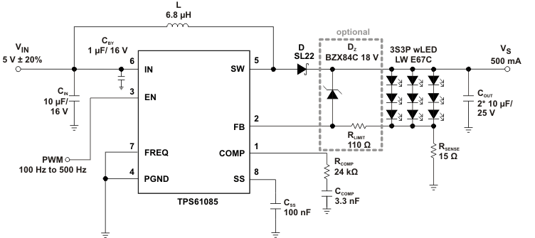 Figure 20. Simple Application (3.3V Input - fsw = 650 kHz) for wLED Supply (3S3P) With Adjustable Brightness Control Using a PWM Signal on the Enable Pin
(With Optional Clamping Zener Diode)
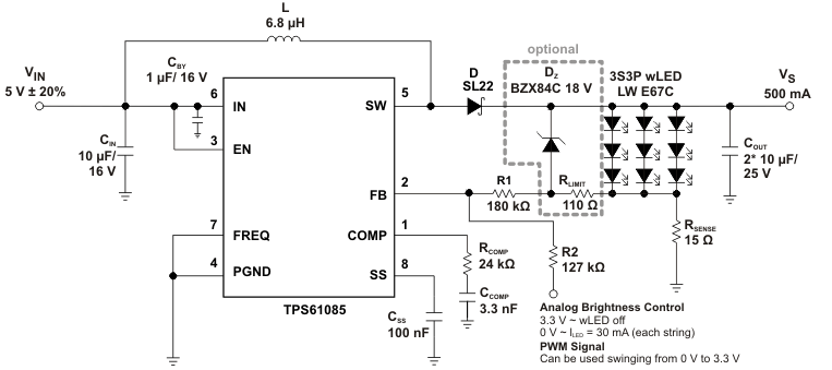 Figure 21. Simple Application (3.3 V Input - fsw = 650 kHz) for wLED Supply (3S3P) With Adjustable Brightness Control Using an Analog Signal on the Feedback Pin
(With Optional Clamping Zener Diode)