SLVS484C June 2003 – December 2014 TPS61090 , TPS61091 , TPS61092
PRODUCTION DATA.
- 1 Features
- 2 Applications
- 3 Description
- 4 Revision History
- 5 Device Comparison Table
- 6 Pin Configuration and Functions
- 7 Specifications
- 8 Parameter Measurement Information
- 9 Detailed Description
-
10Application and Implementation
- 10.1 Application Information
- 10.2
Typical Applications
- 10.2.1 Typical Application Circuit for Adjustable Output Voltage Option
- 10.2.2 TPS6109x Application Schematic of 5 Vout With Maximum Output Power
- 10.2.3 TPS6109x Application Schematic of 5 Vout and Auxiliary 10 Vout With Charge Pump
- 10.2.4 TPS6109x Application Schematic of 5 Vout and Auxiliary -5 Vout With Charge Pump
- 11Power Supply Recommendations
- 12Layout
- 13Device and Documentation Support
- 14Mechanical, Packaging, and Orderable Information
Package Options
Refer to the PDF data sheet for device specific package drawings
Mechanical Data (Package|Pins)
- RSA|16
Thermal pad, mechanical data (Package|Pins)
- RSA|16
Orderable Information
12 Layout
12.1 Layout Guidelines
As for all switching power supplies, the layout is an important step in the design, especially at high peak currents and high switching frequencies. If the layout is not carefully done, the regulator could show stability problems as well as EMI problems. Therefore, use wide and short traces for the main current path and for the power ground tracks. The input capacitor, output capacitor, and the inductor should be placed as close as possible to the IC. Use a common ground node for power ground and a different one for control ground to minimize the effects of ground noise. Connect these ground nodes at any place close to one of the ground pins of the IC.
The feedback divider should be placed as close as possible to the control ground pin of the IC. To lay out the control ground, it is recommended to use short traces as well, separated from the power ground traces. This avoids ground shift problems, which can occur due to superimposition of power ground current and control ground current.
12.2 Layout Example
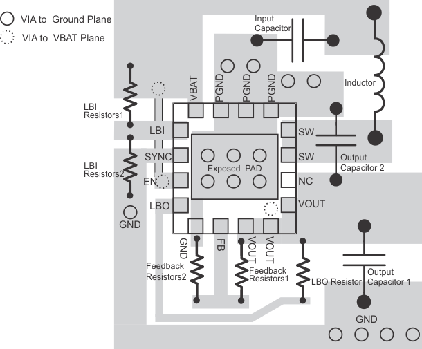 Figure 23. Layout Example Schematic
12.3 Thermal Considerations
Implementation of integrated circuits in low-profile and fine-pitch surface-mount packages typically requires special attention to power dissipation. Many system-dependent issues such as thermal coupling, airflow, added heat sinks and convection surfaces, and the presence of other heat-generating components affect the power-dissipation limits of a given component.
Three basic approaches for enhancing thermal performance are listed below.
- Improving the power dissipation capability of the PCB design
- Improving the thermal coupling of the component to the PCB
- Introducing airflow in the system
The maximum junction temperature (TJ) of the TPS6109x devices is 150°C. The thermal resistance of the 16-pin QFN PowerPAD package (RSA) isRΘJA = 38.1 °C/W, if the PowerPAD is soldered and the board layout is optimized. Specified regulator operation is assured to a maximum ambient temperature TA of 85°C. Therefore, the maximum power dissipation is about 1700 mW. More power can be dissipated if the maximum ambient temperature of the application is lower.
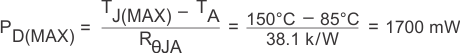
If designing for a lower junction temperature of 125°C, which is recommended, maximum heat dissipation is lower. Using the above equation (8) results in 1050 mW power dissipation.