SLVSFH6C January   2021  – December 2021 TPS61094

PRODUCTION DATA  

  1. Features
  2. Applications
  3. Description
  4. Revision History
  5. Pin Configuration and Functions
  6. Specifications
    1. 6.1 Absolute Maximum Ratings
    2. 6.2 ESD Ratings
    3. 6.3 Recommended Operating Conditions
    4. 6.4 Thermal Information
    5. 6.5 Electrical Characteristics
    6. 6.6 Typical Characteristics
  7. Detailed Description
    1. 7.1 Overview
      1. 7.1.1 The Configuration of VCHG Pin, ICHG Pin, and OSEL Pin
        1. 7.1.1.1 OSEL: Output Voltage Selection
        2. 7.1.1.2 VCHG: Charging Termination Voltage Selection
        3. 7.1.1.3 ICHG: Charging Output Current Selection
    2. 7.2 Functional Block Diagram
    3. 7.3 Feature Description
      1. 7.3.1 Undervoltage Lockout
      2. 7.3.2 Enable and Soft Start
      3. 7.3.3 Active Pulldown for the EN and MODE Pins
      4. 7.3.4 Current Limit Operation
      5. 7.3.5 Output Short-to-Ground Protection
      6. 7.3.6 Thermal Shutdown
    4. 7.4 Device Functional Modes
      1. 7.4.1 Operation Mode Setting
      2. 7.4.2 Forced Bypass Mode Operation
      3. 7.4.3 True Shutdown Mode Operation
      4. 7.4.4 Forced Buck Mode Operation
      5. 7.4.5 Auto Buck or Boost Mode Operation
        1. 7.4.5.1 Three States (Boost_on, Buck_on, and Supplement) Transition
        2. 7.4.5.2 Boost, Bypass, and Pass-Through
        3. 7.4.5.3 PWM, PFM, and Snooze Modes in Boost Operation
          1. 7.4.5.3.1 PWM Mode
          2. 7.4.5.3.2 PFM Mode
          3. 7.4.5.3.3 Snooze Mode
  8. Application and Implementation
    1. 8.1 Application Information
    2. 8.2 Typical Application – 3.6-V Output Boost Converter with Bypass
      1. 8.2.1 Design Requirements
      2. 8.2.2 Detailed Design Procedure
        1. 8.2.2.1 Programming the Output Voltage
        2. 8.2.2.2 Maximum Output Current
        3. 8.2.2.3 Inductor Selection
        4. 8.2.2.4 Output Capacitor Selection
        5. 8.2.2.5 Input Capacitor Selection
      3. 8.2.3 Application Curves
      4. 8.2.4 Typical Application – 3.3-V Output Boost Converter with Automatic Buck or Boost Function
        1. 8.2.4.1 Design Requirements
        2. 8.2.4.2 Detailed Design Procedure
          1. 8.2.4.2.1 Programming the Voltage and Current
        3. 8.2.4.3 Application Curves
  9. Power Supply Recommendations
  10. 10Layout
    1. 10.1 Layout Guidelines
    2. 10.2 Layout Example
  11. 11Device and Documentation Support
    1. 11.1 Device Support
      1. 11.1.1 Third-Party Products Disclaimer
    2. 11.2 Documentation Support
      1. 11.2.1 Related Documentation
    3. 11.3 Receiving Notification of Documentation Updates
    4. 11.4 Support Resources
    5. 11.5 Trademarks
    6. 11.6 Electrostatic Discharge Caution
    7. 11.7 Glossary
  12. 12Mechanical, Packaging, and Orderable Information

Package Options

Mechanical Data (Package|Pins)
Thermal pad, mechanical data (Package|Pins)
Orderable Information

Description

The TPS61094 is a 60-nA IQ boost converter with supercap management. The device provides a power supply solution for smart meter and super capacitor backup power applications.

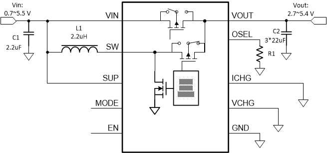
The TPS61094 has a wide input voltage range and output voltage up to 5.5 V. When the TPS61094 works in buck mode and charges the supercap, the charging current and the termination voltage are programmable with two external resistors. When the TPS61094 works in boost mode, the output voltage is programmable with an external resistor.

During automatic buck or boost mode (EN = 1, MODE = 1), when the input power supply is applied, the device bypasses the input voltage to the output while it is capable of charging a backup supercap. When the input power supply is disconnected or lower than the output target voltage, the TPS61094 enters boost mode and regulates output voltage from a backup supercap. The TPS61094 consumes 60-nA quiescent current in this mode.

The TPS61094 supports true shutdown mode (EN = 0, MODE = 1) and the forced bypass mode (EN = 0, MODE = 0). In true shutdown mode, the TPS61094 completely disconnects the load from the input supply. When supporting forced bypass mode, the TPS61094 connects the load to the input voltage directly through a bypass switch and only consumes 4-nA current to achieve long battery life.

Device Information
PART NUMBER PACKAGE(1) BODY SIZE (NOM)
TPS61094 WSON (12) 2.0 mm × 3.0 mm
For all available packages, see the orderable addendum at the end of the data sheet.
Typical Application Circuit 1
GUID-20200831-CA0I-V9L5-NGLG-JSSD3RN4H494-low.gifTypical Application Circuit 2