SLVS791E November   2007  – July 2016 TPS61160 , TPS61161

PRODUCTION DATA.  

  1. Features
  2. Applications
  3. Description
  4. Revision History
  5. Pin Configuration and Functions
  6. Specifications
    1. 6.1 Absolute Maximum Ratings
    2. 6.2 ESD Ratings
    3. 6.3 Recommended Operating Conditions
    4. 6.4 Thermal Information
    5. 6.5 Electrical Characteristics
    6. 6.6 Timing Requirements
    7. 6.7 Typical Characteristics
      1. 6.7.1 Table Of Graphs
  7. Detailed Description
    1. 7.1 Overview
    2. 7.2 Functional Block Diagram
    3. 7.3 Feature Description
      1. 7.3.1 Soft Start-Up
      2. 7.3.2 Open LED Protection
      3. 7.3.3 Current Program
      4. 7.3.4 LED Brightness Dimming Mode Selection
      5. 7.3.5 Undervoltage Lockout
      6. 7.3.6 Thermal Shutdown
    4. 7.4 Device Functional Modes
      1. 7.4.1 Shutdown
      2. 7.4.2 PWM Brightness Dimming
      3. 7.4.3 Digital One-Wire Brightness Dimming
      4. 7.4.4 External PWM Dimming
    5. 7.5 Programming
      1. 7.5.1 EasyScale: One-Wire Digital Dimming
  8. Application and Implementation Information
    1. 8.1 Application Information
    2. 8.2 Typical Applications
      1. 8.2.1 Typical Application of TPS61161
        1. 8.2.1.1 Design Requirements
        2. 8.2.1.2 Detailed Design Procedure
          1. 8.2.1.2.1 Maximum Output Current
          2. 8.2.1.2.2 Inductor Selection
          3. 8.2.1.2.3 Schottky Diode Selection
          4. 8.2.1.2.4 Compensation Capacitor Selection
          5. 8.2.1.2.5 Input and Output Capacitor Selection
        3. 8.2.1.3 Application Curves
      2. 8.2.2 Li-Ion Driver for 6 White LEDs with External PWM Dimming Network
        1. 8.2.2.1 Design Requirements
        2. 8.2.2.2 Detailed Design Procedure
          1. 8.2.2.2.1 Choosing Component Values
        3. 8.2.2.3 Application Curves
      3. 8.2.3 Li-Ion Driver for 6 White LEDs
        1. 8.2.3.1 Design Requirements
        2. 8.2.3.2 Detailed Design Procedure
        3. 8.2.3.3 Application Curves
      4. 8.2.4 Li-Ion Driver for 8 White LEDs
        1. 8.2.4.1 Design Requirements
        2. 8.2.4.2 Detailed Design Procedure
        3. 8.2.4.3 Application Curves
  9. Power Supply Recommendations
  10. 10Layout
    1. 10.1 Layout Guidelines
    2. 10.2 Layout Example
    3. 10.3 Thermal Considerations
  11. 11Device and Documentation Support
    1. 11.1 Device Support
      1. 11.1.1 Third-Party Products Disclaimer
    2. 11.2 Documentation Support
      1. 11.2.1 Related Documentation
    3. 11.3 Related Links
      1. 11.3.1 Related Links
    4. 11.4 Receiving Notification of Documentation Updates
    5. 11.5 Community Resources
    6. 11.6 Trademarks
    7. 11.7 Electrostatic Discharge Caution
    8. 11.8 Glossary
  12. 12Mechanical, Packaging, and Orderable Information

Package Options

Mechanical Data (Package|Pins)
Thermal pad, mechanical data (Package|Pins)
Orderable Information

5 Pin Configuration and Functions

DRV Package
6-Pin WSON with Exposed Thermal Pad
Top View
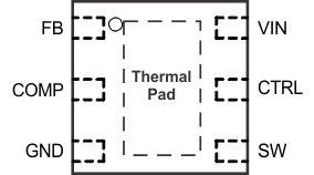
TPS61160 TPS61161 po_lvs791.gif

Pin Functions

PIN I/O DESCRIPTION
NAME NO.
COMP 2 O Output of the transconductance error amplifier. Connect an external capacitor to this pin to compensate the converter.
CTRL 5 I Control pin of the boost converter. It is a multi-functional pin which can be used for enable control, PWM and digital dimming.
FB 1 I Feedback pin for current. Connect the sense resistor from FB to GND.
GND 3 O Ground
SW 4 I This is the switching node of the device. Connect the inductor between the VIN and SW pin. This pin is also used to sense the output voltage for open LED protection
VIN 6 I The input supply pin for the device. Connect VIN to a supply voltage between 2.7 V and 18 V.
Thermal Pad Solder the thermal pad to the analog ground plane. If possible, use thermal via to connect to ground plane for ideal power dissipation.