SLVSB73B December 2011 – May 2015 TPS61165-Q1
PRODUCTION DATA.
- 1 Features
- 2 Applications
- 3 Description
- 4 Revision History
- 5 Pin Configuration and Functions
- 6 Specifications
- 7 Detailed Description
- 8 Application and Implementation
- 9 Power Supply Recommendations
- 10Layout
- 11Device and Documentation Support
- 12Mechanical, Packaging, and Orderable Information
Package Options
Mechanical Data (Package|Pins)
- DBV|6
Thermal pad, mechanical data (Package|Pins)
Orderable Information
8 Application and Implementation
NOTE
Information in the following applications sections is not part of the TI component specification, and TI does not warrant its accuracy or completeness. TI’s customers are responsible for determining suitability of components for their purposes. Customers should validate and test their design implementation to confirm system functionality.
8.1 Application Information
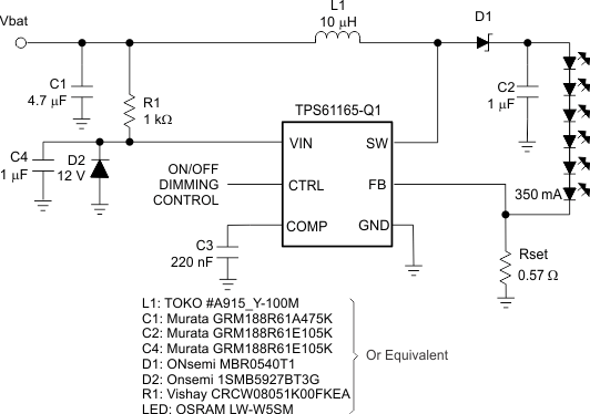
The TPS61165-Q1 device drives 6 high-brightness LEDs; the LED current is set at 350 mA. A 12-V Zener diode is used to clamp the input voltage, which makes the TPS61165-Q1 device suitable for car battery supply applications.
8.2 Typical Application
For assistance in selecting the proper values, the detailed external PWM dimming network for the specific application, see SLVA471 and/or SLVC366.
8.2.1 Design Requirements
Table 4 lists the input parameters for this design example.
Table 4. Design Requirements
| DESIGN PARAMETER | EXAMPLE VALUE |
|---|---|
| Brightness control | PWM Dimming |
| Input voltage | 12 V |
| Output current | 350 mA |
| LED loads | 6 LEDs |
8.2.2 Detailed Design Procedures
8.2.2.1 Maximum Output Current
The overcurrent limit in a boost converter limits the maximum input current and thus maximum input power for a given input voltage. Maximum output power is less than maximum input power due to power conversion losses. Therefore, the current limit setting, input voltage, output voltage and efficiency can all change maximum current output. The current limit clamps the peak inductor current; therefore, the ripple must be subtracted to derive maximum DC current. The ripple current is a function of switching frequency, inductor value and duty cycle. Use Equation 3 and Equation 4 consider of all the above factors for maximum output current calculation.

where
- Ip = inductor peak to peak ripple
- L = inductor value
- Vf = Schottky diode forward voltage
- Fs = switching frequency
- Vout = output voltage of the boost converter. It is equal to the sum of VFB and the voltage drop across LEDs.

where
- Iout_max = Maximum output current of the boost converter
- Ilim = over current limit
- η = efficiency
For instance, when VIN is 3 V, 8 LEDs output equivalent to VOUT of 26 V, the inductor is 22 μH, the Schottky forward voltage is 0.2 V; and then the maximum output current is 110 mA in typical condition. When VIN is 5 V, 10 LEDs output equivalent to VOUT of 32 V, the inductor is 22 μH, the Schottky forward voltage is 0.2 V; and then the maximum output current is 150 mA in typical condition.
8.2.2.2 Inductor Selection
The selection of the inductor affects steady state operation as well as transient behavior and loop stability. These factors make it the most important component in power regulator design. There are three important inductor specifications, inductor value, DC resistance and saturation current. Considering inductor value alone is not enough.
The inductor value determines the inductor ripple current. Choose an inductor that can handle the necessary peak current without saturating, according to half of the peak-to-peak ripple current given by Equation 3, pause the inductor DC current given by:

Inductor values can have ±20% tolerance with no current bias. When the inductor current approaches saturation level, its inductance can decrease 20% to 35% from the 0 A value depending on how the inductor vendor defines saturation current. Using an inductor with a smaller inductance value forces discontinuous PWM when the inductor current ramps down to zero before the end of each switching cycle. This reduces the boost converter’s maximum output current, causes large input voltage ripple and reduces efficiency. Large inductance value provides much more output current and higher conversion efficiency. For these reasons, a 10 μH to 22 μH inductor value range is recommended. A 22 μH inductor optimized the efficiency for most application while maintaining low inductor peak to peak ripple. Table 5 lists the recommended inductor for the TPS61165-Q1 device. When recommending inductor value, the factory has considered –40% and +20% tolerance from its nominal value.
TPS61165-Q1 device has built-in slope compensation to avoid subharmonic oscillation associated with current mode control. If the inductor value is lower than 10 μH, the slope compensation may not be adequate, and the loop can be unstable. Therefore, customers need to verify the inductor in their application if it is different from the recommended values.
Table 5. Recommended Inductors for TPS61165-Q1
| PART NUMBER | L (μH) |
DCR MAX (mΩ) |
SATURATION CURRENT (A) |
SIZE (L × W × H mm) |
VENDOR |
|---|---|---|---|---|---|
| A915_Y-100M | 10 | 90 | 1.3 | 5.2 × 5.2 × 3 | TOKO |
| VLCF5020T-100M1R1-1 | 10 | 237 | 1.1 | 5 × 5 × 2 | TDK |
| CDRH4D22/HP | 10 | 144 | 1.2 | 5 × 5 × 2.4 | Sumida |
| LQH43PN100MR0 | 10 | 247 | 0.84 | 4.5 × 3.2 × 2 | Murata |
8.2.2.3 Schottky Diode Selection
The high switching frequency of the TPS61165-Q1 device demands a high-speed rectification for optimum efficiency. Ensure that the diode’s average and peak current rating exceeds the average output current and peak inductor current. In addition, the reverse breakdown voltage of the diode must exceed the open LED protection voltage. The ONSemi MBR0540 and the ZETEX ZHCS400 are recommended for the TPS61165-Q1 device.
8.2.2.4 Compensation Capacitor Selection
The compensation capacitor C3 (see Functional Block Diagram), connected from COMP pin to GND, is used to stabilize the feedback loop of the TPS61165-Q1 device. A 220-nF ceramic capacitor is suitable for most applications.
8.2.2.5 Input and Output Capacitor Selection
The output capacitor is mainly selected to meet the requirements for the output ripple and loop stability. This ripple voltage is related to the capacitance of the capacitor and its equivalent series resistance (ESR). Assuming a capacitor with zero ESR, the minimum capacitance needed for a given ripple can be calculated using Equation 6.

where
- Vripple = peak-to-peak output ripple
The additional output ripple component caused by ESR is calculated using Equation 7

Due to its low ESR, Vripple_ESR can be neglected for ceramic capacitors, but must be considered if tantalum or electrolytic capacitors are used.
Care must be taken when evaluating a ceramic capacitors derating under DC bias, aging and AC signal. For example, larger form factor capacitors (in 1206 size) have a self resonant frequencies in the range of the switching frequency. So the effective capacitance is significantly lower. The DC bias can also significantly reduce capacitance. Ceramic capacitors can loss as much as 50% of its capacitance at its rated voltage. Therefore, leave the margin on the voltage rating to ensure adequate capacitance at the required output voltage.
The capacitor in the range of 1 μF to 4.7 μF is recommended for input side. The output requires a capacitor in the range of 1 μF to 10 μF. The output capacitor affects the loop stability of the boost regulator. If the output capacitor is below the range, the boost regulator can potentially become unstable.
The popular vendors for high value ceramic capacitors are:
TDK (http://www.component.tdk.com/components.php)
Murata (http://www.murata.com/cap/index.html)
8.2.3 Application Curves
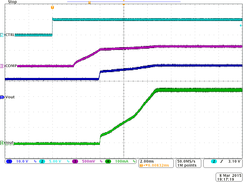
 Figure 16. Start-Up Waveform
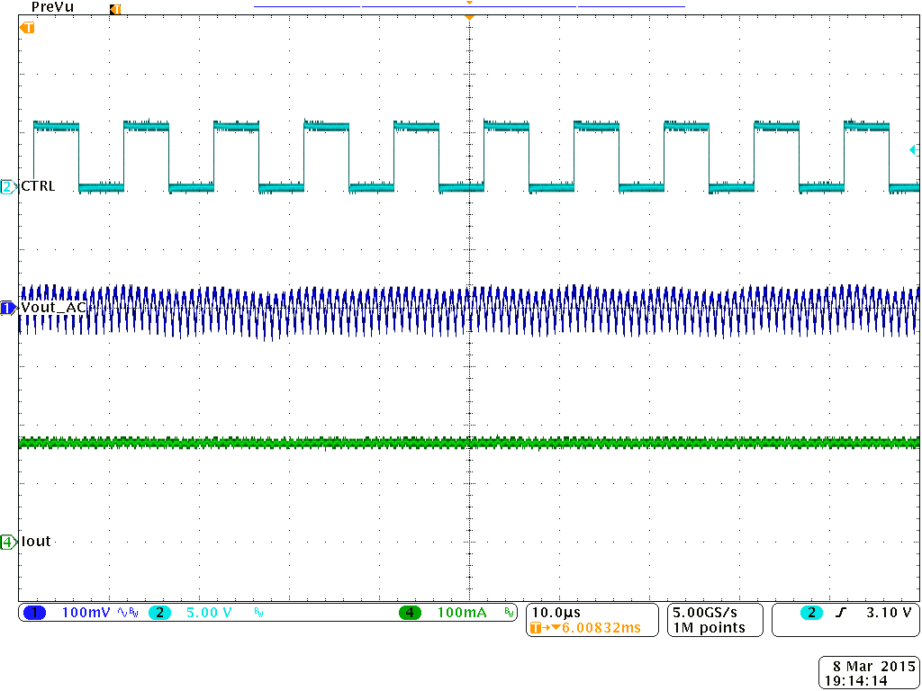
 Figure 17. 100 kHz PWM Dimming Waveform Under 50% Duty Cycle
8.3 Do's and Don'ts
There is a known issue with the TPS61165-Q1 device when using the EasyScale interface to increase the feedback voltage. When VFB is increased from 0 mV to any value more than 0 mV, some ICs do not properly soft-start during this transition and the voltage on their SW pin overshoots. If the overshoot exceeds the absolute maximum voltage rating on the SW pin, the IC is damaged.
With VFB set below 10 mV through EasyScale, the parasitic offsets on the input pins of the internal transconductance amplifier determine the value of output of the amplifier. IC process variations are causing the offset to be larger and in the opposite polarity than expected. If the amplifier’s output is already high before a transition from VFB = 0 mV to any other voltage, then the modulator turns on full, bypassing soft start, and causes the SW pin and output voltage to overshoot.
To avoid this issue do not use EasyScale to change the feedback voltage from 0 mV, effectively disabling the device, to any other voltage. One alternative is to start with VFB = 10 mV and go to a higher voltage. Another alternative is to disable the IC by taking the CTRL pin low for 2.5 ms and then re-enter EasyScale to force a soft start from VFB = 0 mV to the default 200 mV.
