SLVS790E November 2007 – April 2019 TPS61165
PRODUCTION DATA.
- 1 Features
- 2 Applications
- 3 Description
- 4 Revision History
- 5 Device Options
- 6 Pin Configuration and Functions
- 7 Specifications
- 8 Detailed Description
- 9 Application and Implementation
- 10Power Supply Recommendations
- 11Layout
- 12Device and Documentation Support
- 13Mechanical, Packaging, and Orderable Information
Package Options
Mechanical Data (Package|Pins)
Thermal pad, mechanical data (Package|Pins)
- DRV|6
Orderable Information
7.6 Typical Characteristics
Table 1. Table of Graphs
| FIGURE | ||
|---|---|---|
| Efficiency | 3 LEDs (VOUT = 12 V); VIN = 3, 5, 8.5 V; L = 10 μH | Figure 1 |
| Efficiency | 6 LEDs (VOUT = 24 V); VIN = 5, 8.5, 12 V; L = 10 μH | Figure 2 |
| Current limit | TA = 25°C | Figure 3 |
| Current limit | Figure 4 | |
| Easyscale step | Figure 13 | |
| PWM dimming linearity | VIN = 3.6 V; PWM Freq = 10 kHz and 32 kHz | Figure 14 |
| Output ripple at PWM dimming | 3 LEDs; VIN = 5 V; ILOAD = 350 mA; PWM = 32 kHz | Figure 15 |
| Switching waveform | 3 LEDs; VIN = 5 V; ILOAD = 3500 mA; L = 10 μH | Figure 5 |
| Start-up | 3 LEDs; VIN = 5 V; ILOAD = 350 mA; L = 10 μH | Figure 6 |
| Open LED protection | 8 LEDs; VIN = 3.6 V; ILOAD = 20 mA | Figure 7 |
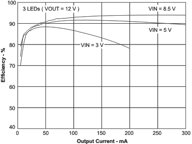 Figure 1. Efficiency vs Output Current
 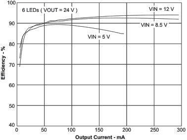 Figure 2. Efficiency vs Output Current
 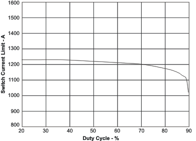 Figure 3. Switch Current Limit vs Duty Cycle
 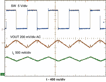 Figure 5. Switching Waveform
 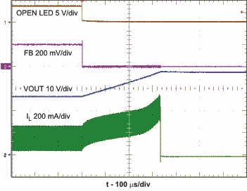 Figure 7. Open LED Protection
 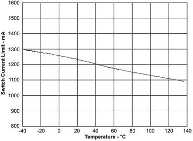 Figure 4. Switch Current Limit vs Temperature
 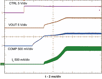 Figure 6. Start-Up