SLVSAN6B February 2011 – September 2016 TPS61181A
PRODUCTION DATA.
- 1 Features
- 2 Applications
- 3 Description
- 4 Revision History
- 5 Device Comparison Table
- 6 Pin Configuration and Functions
- 7 Specifications
- 8 Detailed Description
- 9 Application and Implementation
- 10Power Supply Recommendations
- 11Layout
- 12Device And Documentation Support
- 13Mechanical, Packaging, and Orderable Information
Package Options
Mechanical Data (Package|Pins)
- RTE|16
Thermal pad, mechanical data (Package|Pins)
- RTE|16
Orderable Information
6 Pin Configuration and Functions
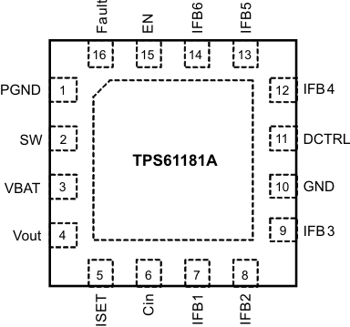
RTE Package
16-Pin WQFN
Top View

Pin Functions
| PIN | I/O | DESCRIPTION | |
|---|---|---|---|
| NO. | NAME | ||
| 1 | PGND | I | Power ground of the device. Internally, it connects to the source of the PWM switch. |
| 2 | SW | I | This pin connects to the drain of the internal PWM switch, external Schottky diode and inductor. |
| 3 | VBAT | I | This pin is connected to the battery supply. It provides the pullup voltage for the Fault pin and battery voltage signal. This is also the input to the internal LDO. |
| 4 | VO | O | This pin monitors the output of the boost regulator. Connect this pin to the anode of the WLED strings. |
| 5 | ISET | I | The resistor on this pin programs the WLED output current. |
| 6 | Cin | I | Supply voltage of the device. It is the output of the internal LDO. Connect 0.1-μF bypass capacitor to this pin. |
| 7, 8, 9 12, 13, 14 |
IFB1-IFB3 IFB4-IFB6 |
I | Current sink regulation inputs. They are connected to the cathode of WLEDs. The PWM loop regulates the lowest VIFB to 400 mV. Each channel is limited to 30-mA current. |
| 10 | GND | I | Signal ground of the device. |
| 11 | DCTRL | I | Dimming control logic input. The dimming frequency range is 100 Hz to 1 kHz. |
| 15 | EN | I | The enable pin to the device. A logic high signal turns on the internal LDO and enables the device. Therefore, do not connect the EN pin to the Cin pin. |
| 16 | Fault | I | Gate driver output for an external PFET used for fault protection. It can also be used as signal output for system fault report. |