SLVSAB4D June 2010 – January 2017 TPS61183
PRODUCTION DATA.
- 1 Features
- 2 Applications
- 3 Description
- 4 Revision History
- 5 Pin Configuration and Functions
- 6 Specifications
-
7 Detailed Description
- 7.1 Overview
- 7.2 Functional Block Diagram
- 7.3 Feature Description
- 7.4
Device Functional Modes
- 7.4.1 Brightness Dimming Control
- 7.4.2 Adjustable PWM Dimming Frequency and Mode Selection (R_FPWM/MODE)
- 7.4.3 Mode Selection - Programmable PWM Dimming or Direct PWM Dimming
- 7.4.4 Direct PWM Dimming
- 7.4.5 Overvoltage Clamp and Voltage Feedback (OVP/FB)
- 7.4.6 Current Sink Open Protection
- 7.4.7 Overcurrent and Short-Circuit Protection
- 7.4.8 Thermal Protection
- 7.4.9 Programmable PWM Dimming
- 8 Application and Implementation
- 9 Power Supply Recommendations
- 10Layout
- 11Device and Documentation Support
- 12Mechanical, Packaging, and Orderable Information
Package Options
Mechanical Data (Package|Pins)
- RTJ|20
Thermal pad, mechanical data (Package|Pins)
- RTJ|20
Orderable Information
7 Detailed Description
7.1 Overview
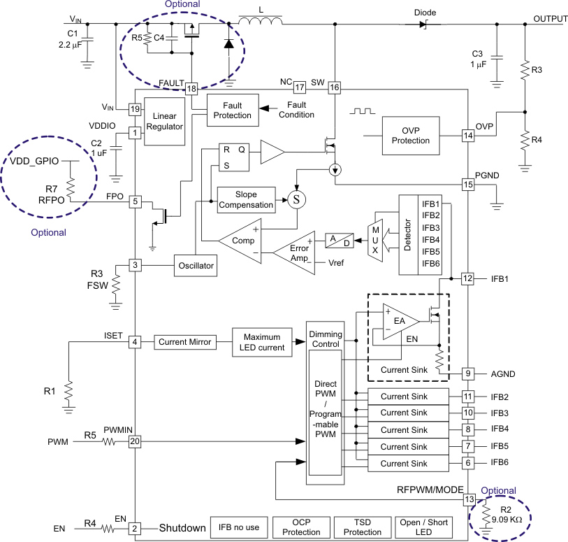
The TPS61183 is a high-efficiency, high output-voltage, white-LED driver for notebook panel backlighting applications. The advantages of white LEDs compared to CCFL backlights are higher power efficiency and lower profile design. Due to the large number of white LEDs required to provide backlighting for medium-to-large display panels, the LEDs must be arranged in parallel strings of several LEDs in series. Therefore, the backlight driver for battery-powered systems is almost always a boost regulator with multiple current sink regulators. For normal operation there must be enough white LEDs in series to ensure the output voltage stays above the input voltage range. Having more white LEDs in series reduces the number of parallel strings, and therefore improves overall current matching. However, the efficiency of the boost regulator declines due to the need for high output voltage.
The TPS61183 device has integrated all of the key function blocks to power and control up to 60 white LEDs. The device includes a 40-V, 2-A boost regulator, six 30-mA current sink regulators, and a protection circuit for overcurrent, overvoltage, open LED, short LED, and output short-circuit failures. The device integrates programmable PWM dimming methods with the PWM interface to control output dimming frequency independently with input frequency. An optional direct PWM mode is user selectable through the RFPWM/MODE selection function.
7.2 Functional Block Diagram
7.3 Feature Description
7.3.1 Supply Voltage
The TPS61183 device has a built-in linear regulator to supply the device analog and logic circuit. The VDDIO pin, output of the regulator, is connected to a 1-µF bypass capacitor for the regulator to be controlled in a stable loop. VDDIO does not have high current sourcing capability for external use but it can be tied to the EN pin for start-up.
7.3.2 Boost Regulator and Programmable Switch Frequency (FSCLT)
The fixed-frequency PWM boost converter uses current-mode control and has integrated loop compensation. The internal compensation ensures stable output over the full input and output voltage ranges assuming the recommended inductance and output capacitance values in Equation 1 are used. The output voltage of the boost regulator is automatically set by the device to minimize voltage drop across the IFB pins. The device regulates the lowest IFB pin to 350 mV and constantly adjusts the boost output voltage to account for any changes in LED forward voltages. If the input voltage is higher than the sum of the white LED forward voltage drops (for example, at low duty cycles), the boost converter is not able to regulate the output due to its minimum duty cycle limitation. In this case, increase the number of WLEDs in series or include series ballast resistors in order to provide enough headroom for the converter to boost the output voltage. Because the TPS61183 integrates a 40-V, 2-A power MOSFET, the boost converter can provide up to a 38-V output voltage.
The TPS61183 switching frequency can be programmed between 280 kHz to 1 MHz by the resistor value on the FSW pin according to Equation 1:

where
- RFSW = FSW pin resistor
See Figure 3 for boost converter switching frequency adjustment resistor RFSW selection.
The adjustable switching frequency feature provides the user with the flexibility of choosing the switching frequency. A faster switching frequency allows for an inductor with smaller inductance and footprint while a slower switching frequency could potentially yield higher efficiency due to lower switching losses. Use Equation 1 or refer to Table 2 to select the correct value:
Table 2. RFSW Recommendations
| RFLCT | ƒSW |
|---|---|
| 833 kΩ | 600 KHz |
| 625 kΩ | 800 KHz |
| 499 kΩ | 1 MHz |
7.3.3 LED Current Sinks
The six current-sink regulators embedded in the TPS61183 can be collectively configured to provide up to a maximum of 30 mA each. These six specialized current sinks are accurate to within ±2% max for currents at 20 mA, with a string-to-string difference of ±1.5% typical.
The IFB current must be programmed to the highest WLED current expected using the ISETH pin resistor and Equation 2.

where
- KISET = 980 (current multiple)
- VISETH = 1.229 V (ISETH pin voltage)
- RISETH = ISETH pin resistor
7.3.4 Enable and Start-Up
The internal regulator which provides VDDIO wakes up as soon as VIN is applied even when EN is low. This allows the device to start when EN is tied to the VDDIO pin; however, VDDIO does not come to full regulation until EN is high. The TPS61183 checks the status of all current feedback channels and shuts down any unused feedback channels. TI recommends shorting the unused channels to ground for faster start-up.
After the device is enabled, if the PWMIN pin is left floating, the output voltage of the TPS61183 regulates to the minimum output voltage. Once the device detects a voltage on the PWMIN pin, the TPS61183 begins to regulate the IFB pin current, as pre-set per the ISETH pin resistor, according to the duty cycle of the signal on the PWMIN pin. The boost converter output voltage rises to the appropriate level to accommodate the sum of the white LED string with the highest forward voltage drops plus the headroom of the current sink at that current.
Pulling the EN pin low shuts down the device, resulting in the device consuming less than 11 µA in shutdown mode.
7.3.5 IFB Pin Unused
The TPS61183 has open/short string detection. For an unused IFB string, simply short it to ground or leave it open. TI recommends shorting unused IFB pins to ground for faster start-up.
7.4 Device Functional Modes
7.4.1 Brightness Dimming Control
The TPS61183 has programmable PWM dimming control with the PWM control interface.
The internal decoder block detects duty cycle information from the input PWM signal, saves it in an eight bit register and delivers it to the output PWM dimming control circuit. The output PWM dimming control circuit turns on/off six output current sinks at the PWM frequency set by RFPWM and the duty cycle from the decoder block.
The TPS61183 also has direct PWM dimming control with the PWM control interface. In direct PWM mode, each current sink turns on/off at the same frequency and duty cycle as the input PWM signal. See Mode Selection – Programmable PWM Dimming or Direct PWM Dimming for dimming mode selection.
When in programmable PWM mode, TI recommends inserting a series resistor of 10-kΩ to 20-kΩ value close to PWMIN pin. This resistor together with an internal capacitor forms a low pass R-C filter with 30-ns to 60-ns time constant. This prevents possible high frequency noises being coupled into the input PWM signal and causing interference to the internal duty cycle decoding circuit. However, it is not necessary for direct PWM mode because the duty cycle decoding circuit is disabled during the direct PWM mode.
7.4.2 Adjustable PWM Dimming Frequency and Mode Selection (R_FPWM/MODE)
The TPS61183 can operate in programmable mode or direct PWM mode. Tying the RFPWM/MODE pin to VDDIO forces the device to operate in direct PWM mode. Alternatively, a resistor between the RFPWM/MODE pin and ground sets the device into programmable mode with the value of the resistor determines the PWM dimming frequency. Use Equation 3 or refer to Table 3 to select the correct value:

where
- RFPWM = RFPWM pin resistor
Table 3. RFPWM Recommendations
| RFPWM | FDIM |
|---|---|
| 866 kΩ | 210 Hz |
| 437 kΩ | 420 Hz |
| 174 kΩ | 1.05 kHz |
| 9.09 kΩ | 20 kHz |
7.4.3 Mode Selection – Programmable PWM Dimming or Direct PWM Dimming
The programmable dimming method or direct PWM dimming method can be selected through the RFPWM/MODE pin. By attaching an external resistor to the RFPWM/MODE pin, the default programmable PWM mode can be selected. To select direct PWM mode, the RFPWM/MODE pin needs to be tied to the VDDIO pin. The RFPWM/MODE pin can be noise sensitive when R2 has high impedance. In this case, careful layout or a parallel bypassing capacitor improves noise sensitivity but the value of the parallel capacitor may not exceed 33 pF for oscillator stability.
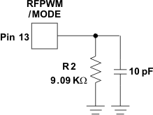 Figure 13. Programmable Dimming Mode Selection
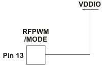 Figure 14. Direct PWM Dimming Mode Selection
7.4.4 Direct PWM Dimming
In direct PWM mode, all current feedback channels are turned on and off and are synchronized with the input PWM signal.
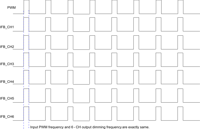 Figure 15. Direct PWM Dimming Timing Diagram
7.4.5 Overvoltage Clamp and Voltage Feedback (OVP/FB)
The overvoltage clamp prevents the boost converter from being damaged due to overvoltage in the event there are no LEDs or failed LEDs in the feedback path. The correct divider ratio is important for optimum operation of the TPS61183. It can be noise sensitive if Rupper and Rdown have high impedance. Careful layout is required. Also, choose lower resistance values for Rupper and Rdown when power dissipation allows. Use the following guidelines to choose the divider value:
- Determine the maximum output voltage, VO, for the system according to the number of series WLEDs.
- Select an Rupper resistor value (1 MΩ for a typical application; a lower value such as 100 kΩ for a noisy environment).
- Calculate Rdown using Equation 4.
- VOV_TH = 1.95 V

where
When the device detects that the OVP pin exceeds 1.95 V typical, indicating that the output voltage is over the set threshold point, the OVP circuitry clamps the output voltage to the set threshold.
7.4.6 Current Sink Open Protection
For the TPS61183, if one of the WLED strings is open, the device automatically detects and disables that string. The device detects the open WLED string by sensing no current in the corresponding IFB pin. As a result, the device deactivates the open IFB pin and removes it from the voltage feedback loop. Subsequently, the output voltage drops and is regulated to the minimum voltage required for the connected WLED strings. The IFB current of the connected WLED strings remains in regulation.
If any IFB pin voltage exceeds the IFB overvoltage threshold (13.5 V typical), the device turns off the corresponding current sink and removes this IFB pin from the regulation loop. The current regulation of the remaining IFB pins is not affected. This condition often occurs when there are several shorted WLEDs in one string. WLED mismatch typically does not create large voltage differences among WLED strings.
The device only shuts down if it detects that all of the WLED strings are open. If an open string is reconnected again, a power-on reset (POR) or EN pin toggling is required to reactivate a previously deactivated string.
7.4.7 Overcurrent and Short-Circuit Protection
The TPS61183 has a pulse-by-pulse over-current limit of 2 A (minimum). The PWM switch turns off when the inductor current reaches this current threshold. The PWM switch remains off until the beginning of the next switching cycle. This protects the deviceand external components during on overload conditions. When there is a sustained overcurrent condition, the device turns off and requires a POR or EN pin toggling to restart. Under severe overload and/or short-circuit conditions, the boost output voltage can be pulled below the required regulated voltage to keep all of the white LEDs operating. Under this condition, the current flows directly from input to output through the inductor and Schottky diode. To protect the TPS61183, the device shuts down immediately. The device restarts after input POR or EN pin toggling.
7.4.8 Thermal Protection
When the junction temperature of the TPS61183 device is over 150°C, the thermal protection circuit is triggered and shuts down the device immediately. Only a POR or EN pin toggling clears the protection and restarts the device.
7.4.9 Programmable PWM Dimming
FDIM is the PWM dimming frequency which is determined by the value of RFPWM on the RFPWM/MODE pin. Figure 16 provides the detailed timing diagram of the programmable PWM dimming mode.
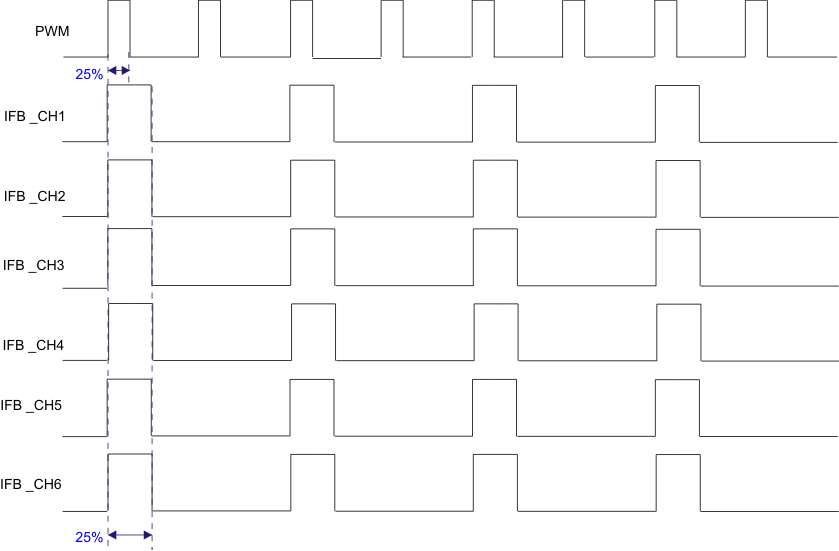 Figure 16. Programmable PWM Dimming Timing Diagram