SLVSAQ2C January 2014 – October 2014 TPS61230 , TPS61232
UNLESS OTHERWISE NOTED, this document contains PRODUCTION DATA.
- 1 Features
- 2 Applications
- 3 Description
- 4 Revision History
- 5 Device Comparison Table
- 6 Pin Configuration and Functions
- 7 Specifications
- 8 Detailed Description
-
9 Applications and Implementation
- 9.1 Application Information
- 9.2
Typical Applications
- 9.2.1 TPS61230 2.3-V to 5.5-V Input, 5-V Output Converter
- 9.2.2 TPS61230 2.3-V to 5.5-V Input, 3.5-V Output Converter
- 9.2.3 TPS61230 Application with Feed Forward Capacitor for Best Transient Response
- 10Power Supply Recommendations
- 11Layout
- 12Device and Documentation Support
- 13Mechanical, Packaging, and Orderable Information
Package Options
Mechanical Data (Package|Pins)
- DRC|10
Thermal pad, mechanical data (Package|Pins)
- DRC|10
Orderable Information
9 Applications and Implementation
NOTE
Information in the following applications sections is not part of the TI component specification, and TI does not warrant its accuracy or completeness. TI’s customers are responsible for determining suitability of components for their purposes. Customers should validate and test their design implementation to confirm system functionality.
9.1 Application Information
The devices are designed to operate from an input voltage supply range between 2.3 V and 5.5 V with a maximum output current of 2.1 A. The devices operate in PWM mode for medium to heavy load conditions and in power save mode at light load currents. In PWM mode the TPS6123x converter operates with the nominal switching frequency of 2 MHz which provides a controlled frequency variation over the input voltage range. As the load current decreases, the converter enters power save mode, reducing the switching frequency and minimizing the IC quiescent current to achieve high efficiency over the entire load current range. The WEBENCH software uses an iterative design procedure and accesses a comprehensive database of components when generating a design. See the Related Documentation section for additional documentation.
9.2 Typical Applications
9.2.1 TPS61230 2.3-V to 5.5-V Input, 5-V Output Converter
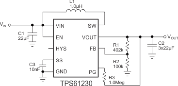 Figure 12. TPS61230 5-V Output Typical Application
9.2.1.1 TPS61230 5-V Output Design Requirements
Use the following typical application design procedure to select external components values for the TPS61230 device.
Table 2. TPS61230 5-V Output Design Parameters
| DESIGN PARAMETERS | EXAMPLE VALUES |
|---|---|
| Input Voltage Range | 2.3 V to 5.5 V |
| Output Voltage | 5.0 V |
| Output Voltage Ripple | ±3% VOUT |
| Transient Response | ±10% VOUT |
| Input Voltage Ripple | ±200 mV |
| Output Current Rating | 2.1 A |
| Operating Frequency | 2 MHz |
9.2.1.2 TPS61230 5-V Detailed Design Procedure
Table 3. TPS61230 5-V Output List of Components
| REFERENCE | DESCRIPTION | MANUFACTURER |
|---|---|---|
| L1 | 1.0 μH, power inductor, XFL4020-102MEB | Coilcraft |
| C1 | 2 μF 6.3 V, 0805, X5R ceramic, GRM21BR60J226ME39 | Murata |
| C2 | 3 × 22 μF 10 V, 0805, X5R ceramic, LMK212BBJ226MG | YUDEN |
| C3 | 10 nF, X7R ceramic | Murata |
| R1 | 402 k, resistor, chip, 1/10W, 1% | Rohm |
| R2 | 100 k, resistor, chip, 1/10W, 1% | Rohm |
9.2.1.2.1 Programming the Output Voltage
The TPS6123x device family's output voltage need to be programmed via an external voltage divider to set the desired output voltage.
An external resistor divider is used, as shown in Equation 5. By selecting R1 and R2, the output voltage is programmed to the desired value. When the output voltage is regulated, the typical voltage at the FB pin is VFB. The following equation can be used to calculate R1 and R2.
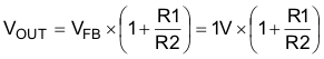
For best accuracy, R2 should be kept smaller than 100 kΩ to ensure that the current following through R2 is at least 100 times larger than FB pin leakage current. Changing R2 towards a lower value increases the robustness against noise injection. Changing the R2 towards higher values reduces the quiescent current for achieving highest efficiency at low load currents.
For the fixed output voltage version, TPS61232, the FB pin must be tied to the output directly.
9.2.1.2.2 Inductor and Capacitor Selection
The second step is the selection of the inductor and capacitor components. To simplify this process, Table 4 outlines possible inductor and output capacitor value combinations.
Table 4. Inductor and Output Capacitor Combinations
| L (µH)(1) | COUT (µF)(2) | ||||
|---|---|---|---|---|---|
| 10 | 20 | 47 | 100 | ||
| 0.47 | √ | √ | √ | ||
| 1.0 | √(3) | √ | √ | ||
| 1.5 | |||||
9.2.1.2.2.1 Inductor Selection
A boost converter requires two main passive components for storing energy during the conversion, an inductor and an output capacitor. It is advisable to select an inductor with a saturation current rating higher than the possible peak current flowing through the power switches. The inductor peak current varies as a function of the load, the input and output voltages and is estimated using Equation 6.
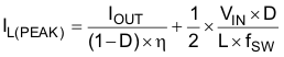
Where
η = Power conversion estimated efficiency
Selecting an inductor with insufficient saturation performance can lead to excessive peak current in the converter. This could eventually harm the device and reduce reliability. It's recommended to choose the saturation current for the inductor 20%~30% higher than the IL(PEAK), from Equation 6. The following inductors are recommended to be used in designs.
Table 5. List of Inductors
| INDUCTANCE [µH] | CURRENT RATING [A] | DC RESISTANCE [mΩ] | PART NUMBER | MANUFACTURER |
|---|---|---|---|---|
| 1.0 | 5.4 | 10.8 | XFL4020-102ME | Coilcraft |
| 1.0 | 7.5 | 9 | LQH6PPN1R0 | muRata |
| 0.47 | 6.6 | 7.6 | XFL4015-471ME | Coilcraft |
9.2.1.2.2.2 Output Capacitor Selection
For the output capacitor, it is recommended to use small X5R or X7R ceramic capacitors placed as close as possible to the VOUT and GND pins of the IC. If, for any reason, the application requires the use of large capacitors which cannot be placed close to the IC, using a smaller ceramic capacitor of 1 µF in parallel to the large one is highly recommended. This small capacitor should be placed as close as possible to the VOUT and GND pins of the IC.
Care must be taken when evaluating a capacitor’s derating under bias. The bias can significantly reduce capacitance. Ceramic capacitors can loss as much as 50% of their capacitance at rated voltage. Therefore, leave margin on the voltage rating to ensure adequate effective capacitance.
The ESR impact on the output ripple must be considered as well, if tantalum or electrolytic capacitors are used. Assuming there is enough capacitance such that the ripple due to the capacitance can be ignored, the ESR needed to limit the VRipple is:

9.2.1.2.2.3 Input Capacitor Selection
Multilayer X5R or X7R ceramic capacitors are an excellent choice for input decoupling of the step-up converter as they have extremely low ESR and are available in small footprints. Input capacitors should be located as close as possible to the device. While a 22-μF input capacitor is sufficient for most applications, larger values may be used to reduce input current ripple without limitations. Take care when using only ceramic input capacitors. When a ceramic capacitor is used at the input and the power is being supplied through long wires, such as from a wall adapter, a load step at the output can induce ringing at the VIN pin. This ringing can couple to the output and be mistaken as loop instability or could even damage the part. Additional "bulk" capacitance (electrolytic or tantalum) should in this circumstance be placed between CIN and the power source to reduce ringing than can occur between the inductance of the power source leads and CIN.
9.2.1.2.3 Loop Stability, Feed Forward Capacitor
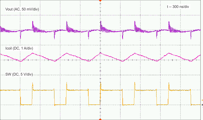
The third step is to check the loop stability. The stability evaluation is to look from a steady-state perspective at the following signals:
- Switching node, SW
- Inductor current, IL
- Output ripple, VRipple(OUT)
When the switching waveform shows large duty cycle jitter or the output voltage or inductor current shows oscillations, the regulation loop may be unstable. This is often a result of board layout and/or L-C combination.
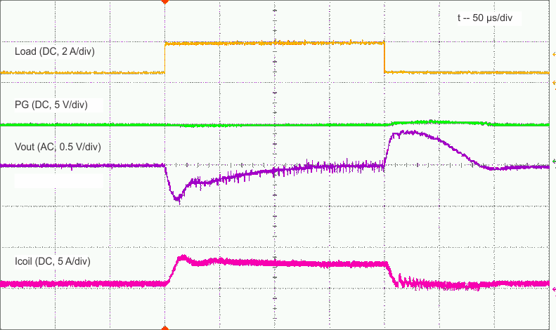
The load transient response is another approach to check the loop stability. During the load transient recovery time, VOUT can be monitored for settling time, overshoot or ringing that helps judge the converter’s stability. Without any ringing, the loop has usually more than 45° of phase margin.
As for the heavy load transient applications such as a 2 A load step transient, a feed forward capacitor in parallel with R1 is recommended. The feed forward capacitor increases the loop bandwidth by adding a zero. This results in a lower output voltage drop, as shown in Figure 36. Set the feed forward capacitor zero near 20 kHz for most applications. See application report Optimizing Transient Response of Internally Compensated dc-dc Converters With Feedforward Capacitor (SLVA289).
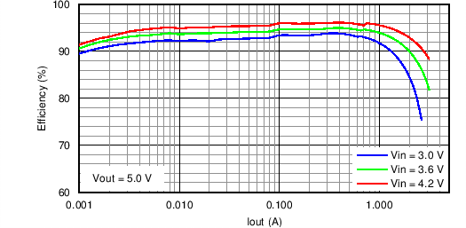
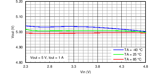
9.2.1.3 TPS61230 5-V Output Application Performance Plots

9.2.2 TPS61230 2.3-V to 5.5-V Input, 3.5-V Output Converter
 Figure 25. TPS61230 3.5-V Output Typical Application
9.2.2.1 TPS61230 3.5-V Output Design Requirements
Table 6. TPS61230 3.5-V Output Design Parameters
| DESIGN PARAMETERS | EXAMPLE VALUES |
|---|---|
| Input Voltage Range | 2.3 V to 5.5 V |
| Output Voltage | 3.5 V |
| Output Voltage Ripple | ±3% VOUT |
| Transient Response | ±10% VOUT |
| Input Voltage Ripple | ±200 mV |
| Output Current Rating | 2.1 A |
| Operating Frequency | 2 MHz |
9.2.2.2 Detailed Design Procedure
Refer to the TPS61230 5-V Detailed Design Procedure section for the 3.5-V detailed design procedures.
9.2.2.3 TPS61230 3.5-V Output Application Performance Plots

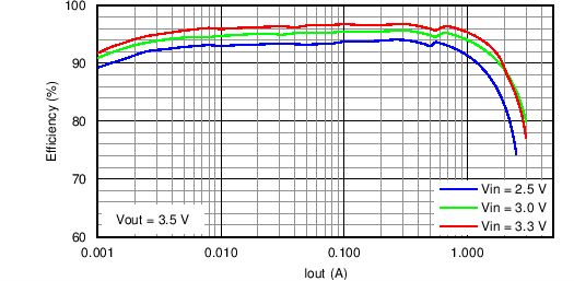

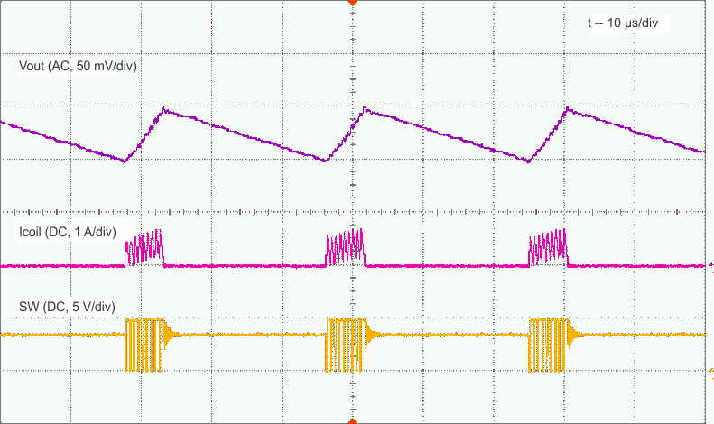
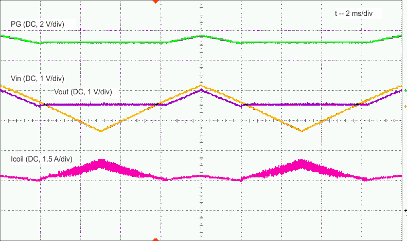 Figure 32. Input Sweep (VOUT = 3.5 V, VIN = 2.7 V to 4.2 V, IOUT = 1.5 A)
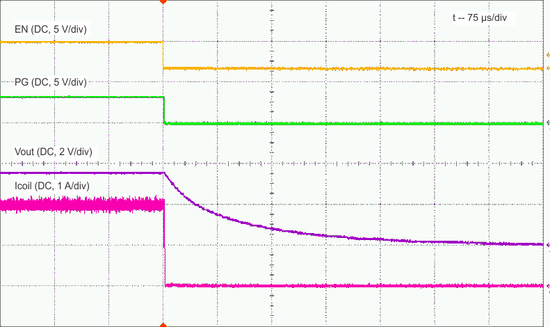 Figure 34. Shutdown (VOUT = 3.5 V, VIN = 3.0 V, ROUT = 2.3 Ω)
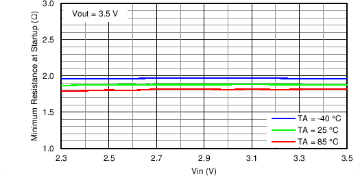
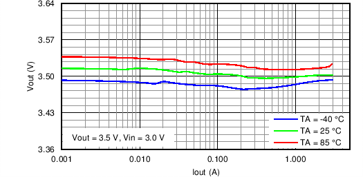
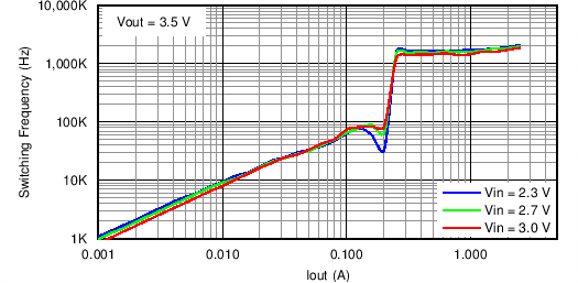
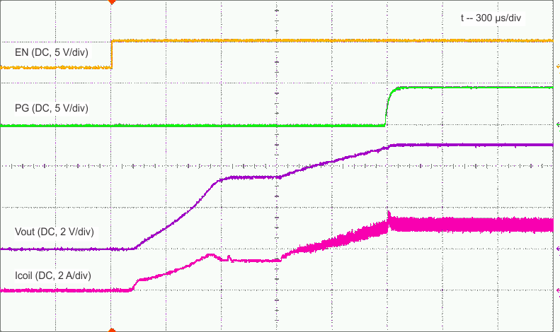
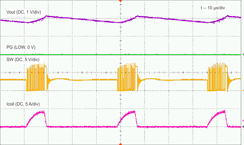
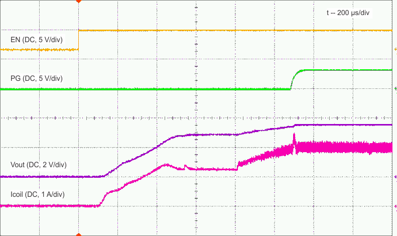 Figure 33. Startup (VOUT = 3.5 V, VIN = 3.0 V, ROUT = 2.3 Ω)
9.2.3 TPS61230 Application with Feed Forward Capacitor for Best Transient Response
As for the heavy load transient applications such as a 2-A load step transient, a feed forward capacitor in parallel with R1 is recommended. The feed forward capacitor increases the loop bandwidth by adding a zero. This results in a lower output voltage drop, as shown in Figure 36. Set the feed forward capacitor zero near 20 kHz for most applications. See application report Optimizing Transient Response of Internally Compensated dc-dc Converters With Feedforward Capacitor (SLVA289).
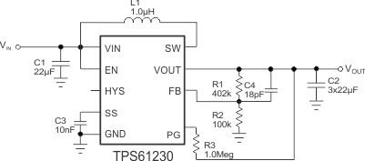 Figure 35. TPS61230 5-V Output with Cff Typical Application
9.2.3.1 Design Requirements
Refer to the TPS61230 5-V Output Design Requirements section for the design requirements.
9.2.3.2 Detailed Design Procedure
Refer to the TPS61230 5-V Detailed Design Procedure section for the detailed design procedures.
9.2.3.3 Application Curve
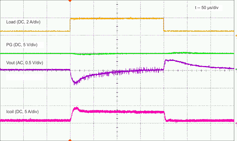 Figure 36. Load Transient (VOUT = 5 V, IOUT = 0.5 A to 2 A, CFF = 18 pF)