SLVSAQ2C January 2014 – October 2014 TPS61230 , TPS61232
UNLESS OTHERWISE NOTED, this document contains PRODUCTION DATA.
- 1 Features
- 2 Applications
- 3 Description
- 4 Revision History
- 5 Device Comparison Table
- 6 Pin Configuration and Functions
- 7 Specifications
- 8 Detailed Description
-
9 Applications and Implementation
- 9.1 Application Information
- 9.2
Typical Applications
- 9.2.1 TPS61230 2.3-V to 5.5-V Input, 5-V Output Converter
- 9.2.2 TPS61230 2.3-V to 5.5-V Input, 3.5-V Output Converter
- 9.2.3 TPS61230 Application with Feed Forward Capacitor for Best Transient Response
- 10Power Supply Recommendations
- 11Layout
- 12Device and Documentation Support
- 13Mechanical, Packaging, and Orderable Information
Package Options
Mechanical Data (Package|Pins)
- DRC|10
Thermal pad, mechanical data (Package|Pins)
- DRC|10
Orderable Information
7 Specifications
7.1 Absolute Maximum Ratings
over operating free-air temperature range (unless otherwise noted)(1)| MIN | MAX | UNIT | ||
|---|---|---|---|---|
| Voltage range at pins(2) | EN, FB, PG, SS, HYS, VIN, VOUT, SW | –0.3 | 7 | V |
| Operating junction temperature range, TJ | –40 | 150 | °C | |
(1) Stresses beyond those listed under absolute maximum ratings may cause permanent damage to the device. These are stress ratings only, and functional operation of the device at these or any other conditions beyond those indicated under recommended operating conditions is not implied. Exposure to absolute-maximum-rated conditions for extended periods my affect device reliability.
(2) All voltages are with respect to network ground pin.
7.2 Handling Ratings
| MIN | MAX | UNIT | |||
|---|---|---|---|---|---|
| Tstg | Storage temperature range | -65 | 150 | °C | |
| VESD | Electrostatic discharge | Human body model (HBM), per ANSI/ESDA/JEDEC JS-001, all pins(1) | –2 | 2 | kV |
| Charged device model (CDM), per JEDEC specification JESD22-C101, all pins(2) | –500 | 500 | V | ||
(1) JEDEC document JEP155 states that 500-V HBM allows safe manufacturing with a standard ESD control process.
(2) JEDEC document JEP157 states that 250-V CDM allows safe manufacturing with a standard ESD control process.
7.3 Recommended Operating Conditions
| MIN | TYP | MAX | UNIT | ||||
|---|---|---|---|---|---|---|---|
| VIN | Supply voltage at VIN pin | 2.3 | 5.5 | V | |||
| ISINK_PG | Sink current at PG pin | 500 | µA | ||||
| VPG | Pull-up resistor voltage | 5.5 | V | ||||
| TJ | Operating junction temperature | -40 | 125 | °C | |||
7.4 Thermal Information
| THERMAL METRIC(1) | TPS6123x | UNIT | |
|---|---|---|---|
| DRC (11 PINS) | |||
| RθJA | Junction-to-ambient thermal resistance | 49.1 | °C/W |
| RθJC(top) | Junction-to-case(top) thermal resistance | 57.2 | |
| RθJB | Junction-to-board thermal resistance | 26.6 | |
| ψJT | Junction-to-top characterization parameter | 0.8 | |
| ψJB | Junction-to-board characterization parameter | 23.8 | |
| RθJC(bottom) | Junction-to-case(bottom) thermal resistance | 4.5 | |
(1) For more information about traditional and new thermal metrics, see the IC Package Thermal Metrics application report, SPRA953.
7.5 Electrical Characteristics
TJ = –40°C to 125°C and VIN = 3.6 V. Typical values are at TJ = 25°C, unless otherwise noted.| PARAMETER | TEST CONDITIONS | MIN | TYP | MAX | UNIT | ||
|---|---|---|---|---|---|---|---|
| SUPPLY | |||||||
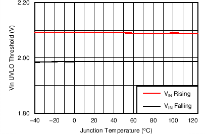
| VUVLO | Input under voltage lockout | VIN falling | 2.0 | 2.1 | V | ||
| VIN rising | 2.1 | 2.2 | |||||
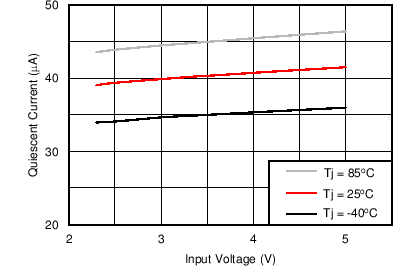
| IQ | Quiescent current into VIN | IC enabled, No load, No switching VOUT = 5 V, TJ = –40 °C to 85°C |
35 | 60 | µA | ||
| IC enabled, No load VIN = 4.2 V, VOUT = No supply, TJ = –40 °C to 85°C |
200 | 230 | |||||
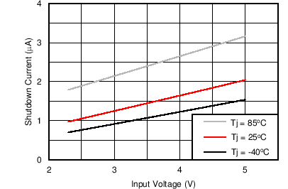
| ISD | Shutdown current into VIN | 0 V ≤ VEN ≤ 0.4 V, VIN = 2.3 V to 5.5 V, TJ = -40 °C to 85°C | 1.5 | 6 | µA | ||
| Leakage current from SW to VOUT | VEN = 0 V, VOUT = 0 V; VSW = VIN = 3.6 V | 2.5 | µA | ||||
| OUTPUT | |||||||
| VOUT | Output voltage range | 2.5 | 5.5 | V | |||
| VOUT | Output voltage accuracy, TPS61232 | PWM mode | 4.9 | 5.0 | 5.1 | V | |
| VOUT | Output voltage accuracy, TPS61232 | PFM mode(1) | 5.035 | V | |||
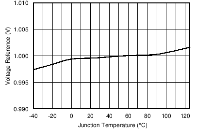
| VFB | Feedback voltage, TPS61230 and TPS61231 | PWM mode | 0.985 | 1 | 1.015 | V | |
| PFM mode(1) | 1.007 | ||||||
| FB pin leakage current | VFB = 1 V | 100 | nA | ||||
| RDIS | Output discharge resistor TPS61231 |
VOUT = 5 V | 200 | Ω | |||
| VOVP | Over voltage protection DC threshold | VOUT rising | 5.7 | 6 | 6.2 | V | |
| Over voltage protection hysteresis | VOUT falling below VOVP | 0.15 | |||||
| ISS | Bias current in soft start phase | After pre-charge phase | 5 | µA | |||
| Line regulation | IOUT = 1 A, VIN = 2.3 V to 4.5 V | 0.06 | %/V | ||||
| Load regulation | IOUT = 0.5 A to 2 A | 0.15 | %/A | ||||
| LOGIC INTERFACE | |||||||
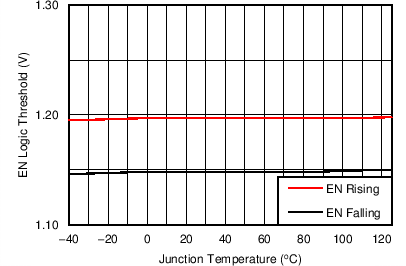
| VTH_EN_ON | EN pin threshold rising | VIN = 2.3 V to 5.5 V | 1.15 | 1.19 | 1.23 | V | |
| VTH_EN_OFF | EN pin threshold falling | VIN = 2.3 V to 5.5 V | 1.11 | 1.14 | 1.18 | V | |
| VOL_HYS | HYS pin low level voltage | ISINK_HYS = 1 mA, VEN = 1.1 V | 0.7 | V | |||
| VTH_PG | Power good DC threshold | VOUT rising, referenced to VOUT_NOMINAL | 93% | 95% | 99% | ||
| VOUT falling referenced to VOUT_NOMINAL | 87% | 90% | 93% | ||||
| VOL_PG | PG pin low level voltage | ISINK_PG = 500 µA | 0.4 | V | |||
| POWER STAGE | |||||||
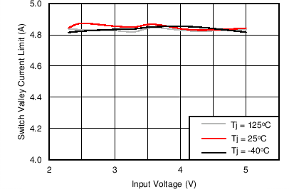
| ILIM_SW | Switch valley current limit | 4.0 | 5.0 | 6.0 | A | ||
| ILIM_Pre | Precharge current limit | VOUT = 5 V | 2.0 | 2.8 | 3.5 | A | |
| VOUT = 3.5 V | 1.8 | 2.6 | 3.3 | ||||
| VOUT = 0 V | 0.4 | 0.55 | 0.7 | ||||
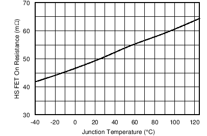
| RDS(on) | High side MOSFET on resistance | VOUT = 5 V | 50 | 75 | mΩ | ||
| Low side MOSFET on resistance | VOUT = 5 V | 50 | 75 | ||||
| TJSD | Thermal shutdown threshold | TJ rising | 150 | °C | |||
| Thermal shutdown hysteresis | TJ falling below TJSD | 20 | |||||
(1) L = 1 µH, COUT = 20 µF (effective capacitance value)
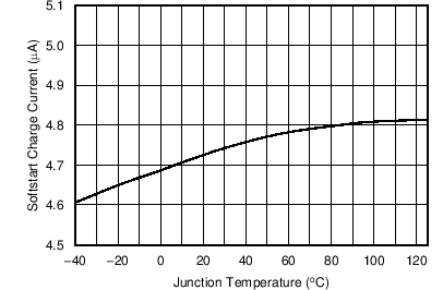
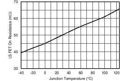
7.6 Typical Characteristics
VIN = 3.6 V, VOUT = 5.0 V, TJ = -40°C to 125 °C, unless otherwise noted.