SLVSCK4A September 2015 – May 2016 TPS61235P , TPS61236P
PRODUCTION DATA.
- 1 Features
- 2 Applications
- 3 Description
- 4 Revision History
- 5 Device Comparison Table
- 6 Pin Configuration and Functions
- 7 Specifications
-
8 Detailed Description
- 8.1 Overview
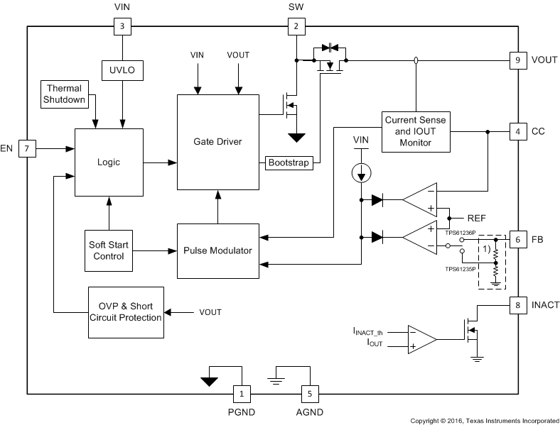
- 8.2 Functional Block Diagram
- 8.3
Feature Description
- 8.3.1 Boost Controller Operation
- 8.3.2 Soft Start
- 8.3.3 Enable and Disable
- 8.3.4 Constant Output Voltage and Constant Output Current Operations
- 8.3.5 Over Current Protection
- 8.3.6 Load Status Indication
- 8.3.7 Under voltage Lockout
- 8.3.8 Over Voltage Protection and Reverse Current Block
- 8.3.9 Short Circuit Protection
- 8.3.10 Thermal Shutdown
- 8.4 Device Functional Modes
-
9 Applications and Implementation
- 9.1 Application Information
- 9.2
Typical Applications
- 9.2.1
TPS61236P 3-V to 4.35-V Input, 5-V Output Voltage, 3-A Maximum Output Current
- 9.2.1.1 Design Requirements
- 9.2.1.2 Detailed Design Procedure
- 9.2.1.3 TPS61236P 5-V Output Application Curves
- 9.2.2 TPS61236P 2.3-V to 5-V Input, 5-V 2-A Output Converter
- 9.2.1
TPS61236P 3-V to 4.35-V Input, 5-V Output Voltage, 3-A Maximum Output Current
- 10Power Supply Recommendations
- 11Layout
- 12Device and Documentation Support
- 13Mechanical, Packaging, and Orderable Information
Package Options
Mechanical Data (Package|Pins)
- RWL|9
Thermal pad, mechanical data (Package|Pins)
Orderable Information
8 Detailed Description
8.1 Overview
The TPS6123x is a high current, high efficiency synchronous boost converter with constant current output feature. It is optimized for single cell Li-Ion and Li-polymer battery powered products, in a wide range of power bank, tablet, and other portable devices. The converter integrates 14-mΩ /14-mΩ power switches and is capable of delivering more than 3.5-A output current for 3.3-V to 5-V conversion. The low Rds(on) of the internal power switches enables up to 97% power conversion efficiency.
The TPS6123x has two regulation loops, one is the output voltage regulation loop as the normal boost converters have, and the other is the output current regulation loop. An external resistor can be used to program the maximum output current, and once the output current reaches the programmed value, the current loop kicks in to regulate the output current. The TPS6123x can also indicate the load status. These features can simplify system design, eliminate external power path components like a load switch, and achieve much lower system thermal dissipation and improve the total power conversion effectively.
The TPS6123x also consumes only 10-µA quiescent current under a light load condition. This low quiescent current together with the load status indication function makes the device very suitable for Always-On applications. For example, for a power bank application, the TPS6123x can remain always on and report load status to the system controller.
8.2 Functional Block Diagram

8.3 Feature Description
8.3.1 Boost Controller Operation
The TPS6123x synchronous boost converter typically operates at a quasi-constant 1-MHz frequency Pulse Width Modulation (PWM) at moderate to heavy load, which allows the use of small inductors and capacitors to achieve a small solution size. At light load, it operates in power-save mode with Pulse Frequency Modulation (PFM) for improved efficiency.
During PWM operation, the converter uses a quasi-constant on-time valley current mode control scheme to achieve excellent line/load regulation. Based on the VIN /VOUT ratio, a simple circuit predicts the required on-time. At the beginning of the switching cycle, the low-side NMOS switch is turned on and the inductor current ramps up to a peak current that is determined by the on-time and the inductance. Once the on-time has expired, the low-side switch is turned off and the rectifying NMOS switch is turned on. The inductor current decays until reaching the valley current threshold which is determined by internal control loops. Once this occurs, the on-time is set again to turn the low-side switch back on and the cycle is repeated. Internal loop compensation is implemented to simplify the design process while minimizing the number of external components. A bootstrap circuit is built in to drive the rectifying NMOS switch. Figure 13 illustrates the PWM mode operation.
 Figure 13. PWM Mode Operation Illustration
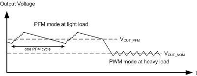
Under a light load condition, the converter works in Pulse Frequency Modulation (PFM) mode. In this mode, the boost converter switches and ramps up the output voltage until VOUT reaches the PFM threshold. Then it stops switching and consumes less quiescent current. It resumes switching when the output voltage drops below the threshold. The converter exits PFM mode when the output current can no longer be supported in this mode. Refer to Figure 14 for PFM mode operation details.
 Figure 14. PFM Mode Operation Illustration
8.3.2 Soft Start
The TPS6123x integrates an internal soft start circuit which controls ramp up of the output voltage and prevents the converter from inrush current during start-up.
When the device is enabled, the rectifying switch is turned on to charge the output capacitor to the input voltage. This is called the pre-charge phase. During the phase, the output current is limited to the pre-charge current limit ILIM_pre, which is proportional to the output voltage. The pre-charge current increases when the output voltage gets higher.
Once the output capacitor is charged close to the input voltage, the converter starts switching. This is called the start-up switching phase. During the phase, the converter steps up the voltage to its nominal output voltage by following an internal ramp up reference voltage, which ramps up in around 3 ms (typ.) to its final value. The current limit function is activated in this phase.
Because of the current limitation during the pre-charge phase, the TPS6123x may not be able to start up under a heavy load condition. It is recommended to apply no load or a light load during the startup process, and apply the full load only after the TPS6123x starts up successfully. Refer to Figure 8 for the recommended minimum load resistance.
8.3.3 Enable and Disable
An external logic signal at the EN pin can enable and disable the device.
The TPS6123x device starts operation when EN is set high and starts up with the soft-start process. For proper operation, the EN pin must be terminated and must not be left floating. Pulling EN low forces the device into shutdown, with a shutdown current of typically 0.01 µA. In shutdown mode, a true disconnection between input and output is implemented. It can prevent current from input to output, or reverse current from output to input.
8.3.4 Constant Output Voltage and Constant Output Current Operations
Normally a boost converter only regulates its output voltage, but for the TPS6123x, it is different. There are two regulation loops for the device. One loop regulates the output voltage, and it is called CV (Constant Voltage) operation; the other regulates the output current, and it is called CC (Constant Current) operation.
8.3.4.1 Constant Voltage Operation
Before the output current reaches the constant current value programmed by an external resistor at the CC pin, the voltage regulation loop dominates. The output voltage is monitored via external or internal feedback network resistors at the FB pin. An error amplifier compares the feedback voltage to an internal reference voltage VREF and adjusts the inductor current valley accordingly. In this way, the TPS6123x operates as a normal boost converter to regulate the output voltage.
During CV operation, the maximum VIN should be 0.6-V below VOUT to keep the output voltage well regulated. The TPS6123x may enter into pass-through operation prematurely when VIN is close to but still below VOUT, and exists when VIN is below the threshold with a hysteresis. When in pass-through operation, the boost converter stops switching and keeps the rectifying switch on, so the input voltage can pass through the external inductor and internal rectifying switch to the output. The output current capability becomes lower and is limited by the pre-charge current limit ILIM_pre of the rectifying switch. More than 0.4-V under-voltage of VOUT may occur due to the premature pass-through operation and the hysteresis of existing. If the under-voltage is not acceptable, the maximum VIN should be limited to 0.6-V below VOUT , which gives enough margin to avoid the pass-through operation.
8.3.4.2 Output Current Monitor
During the CV operation, the output current can be monitored at the CC pin. In the TPS6123x, the inductor current is sensed through the rectifying switch during the off-time of each switching cycle. The device then builds a current signal which is 1/K times the sensed current and feeds it to the CC pin during off-time. As a result, the CC pin voltage, VCC, is proportional to the average output current as Equation 1 shows.

Where:
VCC is the voltage at the CC pin,
IOUT is the output current,
K is the coefficient between the output current and the internal built current signal, K = 100,000,
RCC is the resistor connected at the CC pin.
A capacitor must be connected in parallel with RCC to average the CC pin voltage and also stabilize the control loop. Normally a 10-nF capacitor is recommended. A larger capacitor at the CC pin will smooth the CC voltage better, and also slow down the loop response.
The CC pin can be connected to ground to disable the output current monitor function, and it will not affect the CV operation.
8.3.4.3 Constant Current Operation
As Equation 1 shows, the CC pin voltage is proportional to the output current. The TPS6123x monitors the CC pin voltage and compares it to an internal reference voltage VREF, which is 1.244 V typically. When VCC exceeds VREF, the CC regulation loop kicks in and pulls the inductor current valley to a lower value so to keep the CC pin voltage at VREF. Equally, the output current is regulated at the set value as Equation 2.

Where:
IOUT_CC is the set constant output current,
VREF is the internal reference voltage, 1.244 V typically,
RCC is the resistor connected at the CC pin,
K is the coefficient between the output current and the internal built current signal, K = 100,000.
If the load current is higher than the CC setting, the output voltage drops. A balance can be achieved if the load decreases and matches the CC current before VOUT is pulled below input voltage. In the balance status, the TPS6123x can keep CC operation, output the constant current, and maintain the output voltage at the balanced level. If the output voltage is pulled below the input voltage by a strong load before the balance is achieved, the device exits CC operation and enters into start-up process, where the output current is limited by ILIM_pre instead of the CC value. If the load is still higher than ILIM_pre, the device will be stuck in the pre-charge phase; otherwise, the device can complete the pre-charge phase, but its output voltage will be pulled down again in the switching phase due to the limited output current, so an oscillation may happen.
In order to avoid the potential oscillation, the CC operation is only recommended for pure resistive loads or load devices with dynamic power management function. For a resistive load, its resistance should be higher than VIN / IOUT_CC; for a load device with dynamic power management function, which can regulate its input voltage to a set value, a higher set voltage than VIN of the TPS6123x is suggested. By doing this, a balance can be achieved before the output voltage is pulled below the input voltage, so to avoid the TPS6123x entering into the startup process.
For effective CC operation, a capacitor must be connected in parallel with RCC at CC pin, and the CC value should be set lower than the maximum output capability of the converter; otherwise, the TPS6123x will trigger the over current protection first and fail to regulate the output current. Refer to the Over Current Protection section for details.
The CC operation can be disabled by shorting the CC pin to ground. By doing so, the CC loop is disabled, so the TPS6123x works as a normal boost converter to regulate the output voltage, and its maximum output current capability is decided by the internal current limit.
8.3.5 Over Current Protection
To protect the device from over load condition, an internal cycle-by-cycle current limit is implemented. Once the inductor valley current reaches the internal current limit, the protection is triggered and it clamps the valley current at the limit ILIM until next cycle comes.
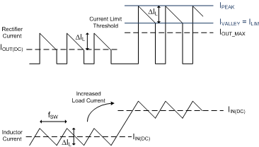
Figure 15 illustrates the valley current limit scheme. The average of the rectifier ripple current equals the output current, IOUT(DC). When the load current increases, the loop increases the valley current accordingly. If the valley current is increased above ILIM, the off-time will be extended until the valley drops to ILIM. Then the next cycle begins.
 Figure 15. Current Limit Operation
The maximum output current, IOUT_MAX, before the device enters into over current protection is decided by its operation condition and the switch current limit threshold. It can be calculated by using the following equations.


Where:
D is the duty cycle of the boost converter,
ILIM is the switch valley current limit threshold,
ΔIL is the inductor current ripple,
L is the inductor value,
fSW is the switching frequency,
η is the conversion efficiency under the operation condition.
To estimate the maximum output current capability in the worst case, the minimum input voltage value, highest fSW value, and minimum ILIM value should be used for the calculation. And η should be the efficiency under this minimum VIN operation condition.
When the current limit is reached, the output voltage decreases during further load increases. If the output voltage drops below the input voltage, the device enters into the start-up process.
8.3.6 Load Status Indication
The TPS6123x can indicate load status by the INACT pin. The INACT pin is an open drain output and should be connected to a pull-up resistor. The INACT pin outputs high impedance when the boost converter works under inactive status (no load or light load status), and it outputs low logic when the boost converter works under active status (moderate load or heavy load status).
Load status is defined by operation mode and output current. When the converter works in PFM mode with IOUT lower than the threshold IINACT_th for 16 PFM cycles, the boost enters inactive status. One PFM cycle is defined from the time the boost starts switching to ramp up the output voltage to the time it resumes switching after the output voltage drops below the PFM threshold, as shown in Figure 14. Once the output current is detected higher than IINACT_th or the converter exits PFM mode, the boost enters active status. There is 10-ms typical deglitch time when the INACT pin changes its output.
This indication function can report load status to a system controller, like an MCU. For example, it can be used to realize the load insert detection in a power bank application, where the TPS6123x can be kept always on while consuming only 10-µA quiescent current. When a load is applied, the TPS6123x detects the load and pulls the INACT pin low to wake up the MCU. It eliminates the need for external load detection circuitry and simplifies the system design.
8.3.7 Under voltage Lockout
Under voltage lockout prevents operation of the device at input voltages below typical 2.1-V. When the input voltage is below the under voltage threshold, the device is shut down and the internal switch FETs are turned off. If the input voltage rises by under voltage lockout hysteresis, the IC restarts.
8.3.8 Over Voltage Protection and Reverse Current Block
When the device detects the output voltage above the threshold VOVP, the over voltage protection will be triggered. The device stops switching and turn off the low side switch and rectifying switch. The voltage at output is blocked to input, and there is no reverse current. When the output voltage falls below the OVP threshold, the device resumes normal operation.
8.3.9 Short Circuit Protection
If the output voltage is detected lower than the input voltage during operation, the TPS6123x will enter into the pre-charge phase of the startup process. The output current is limited to ILIM_pre by the rectifying switch, which is 0.25-A typical when VOUT is short to ground. When the short circuit event is removed, the TPS6123x will start up automatically.
Short circuit protection is only valid when the input voltage is below 4.5 V. If the input voltage is higher than 4.5 V, a long term short to ground event may damage the device.
8.3.10 Thermal Shutdown
The TPS6123x has a built-in temperature sensor which monitors the internal junction temperature, TJ. If the junction temperature exceeds the threshold (140°C typical), the device goes into thermal shutdown, and the high-side and low-side MOSFETs are turned off. When the junction temperature falls below the thermal shutdown minus its hysteresis (15°C typical), the device resumes operation.
8.4 Device Functional Modes
8.4.1 PWM Mode
The TPS6123x boost converter operates at a quasi-constant 1-MHz frequency PWM mode at moderate to heavy load currents. Refer to the Boost Controller Operation section for details.
8.4.2 PFM Mode
The TPS6123x works in PFM mode under light load conditions to improve light load efficiency. Refer to the Boost Controller Operation section for details.
8.4.3 CV Mode and CC Mode
A resistor at the CC pin can program the maximum output current of the TPS6123x. Before the output current reaches the programmed value, the TPS6123x works in CV (Constant Voltage) mode as a normal boost converter. When the output current reaches the programmed value, the TPS6123x works in CC (Constant Current) mode. Refer to the Constant Output Voltage and Constant Output Current Operations section for details.